


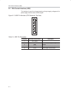
PWM Timing, Interchannel Delay Registers
2-8
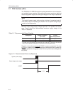
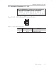
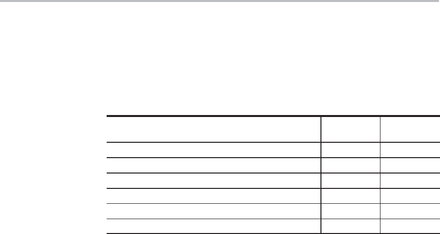
2.6 PWM Timing, Interchannel Delay Registers
For maximum performance, the PWM timing must be optimized for the specific
configuration and PCB layout. The default values in TAS5066 is properly not
optimal in many designs and therefore the interchannel delays must be pro-
grammed by I2C to the TAS5066 at startup and after every system reset.
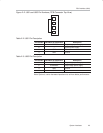
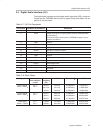
Table 2−9.Recommended Interchannel Delay Register Values (based on EVM designs)
Register Description Register
Address
Value (hex)
Inter−Channel Delay Channel 1 0x0C 0x01
Inter−Channel Delay Channel 2 0x0D 0x49
Inter−Channel Delay Channel 3 0x0E 0x91
Inter−Channel Delay Channel 4 0x0F 0xD9
Inter−Channel Delay Channel 5 0x10 0x21
Inter−Channel Delay Channel 6 0x11 0x69