PSU Interface (J901)
2-3
System Interfaces
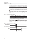
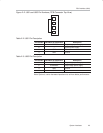
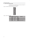
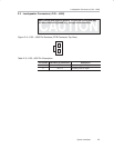
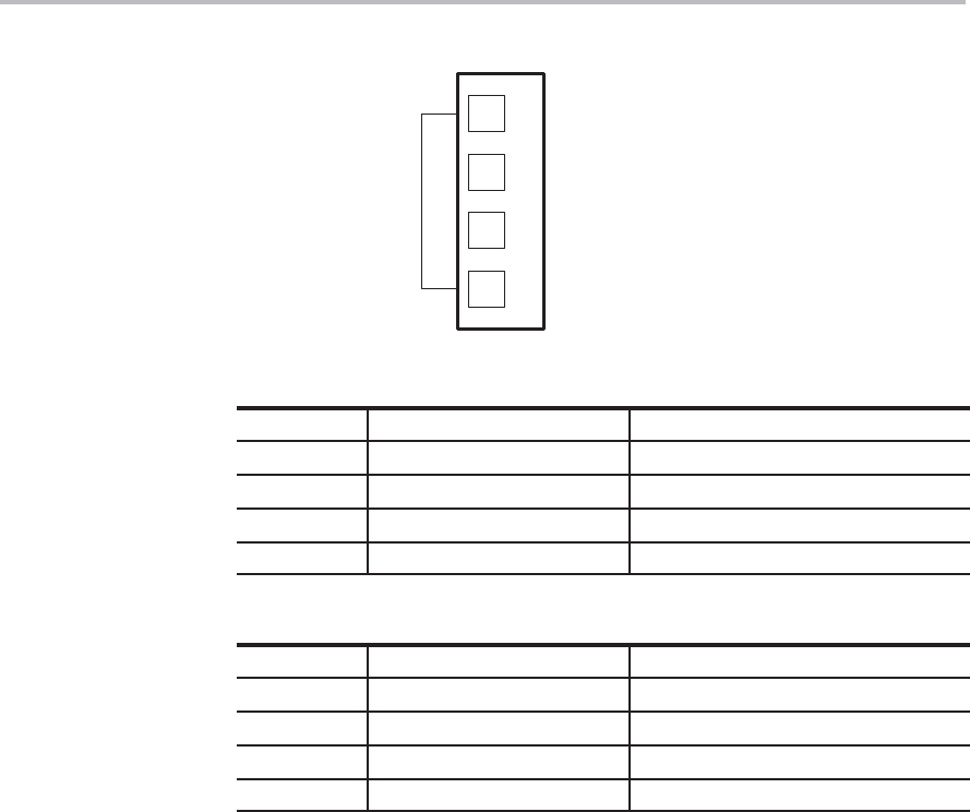
Figure 2−2. J901 and J903 Pin Numbers (PCB Connector Top View)
4
3
2
1
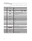
Table 2−2.J901 Pin Description
Pin Number Net-Name at Schematics Description
1 V-HBRIDGE Output stage power supply
2 − System power supply
3 GND Ground
4 GND Ground
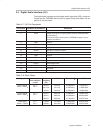
Table 2−3.J903 Pin Description
Pin Number Net-Name at Schematics Description
1 V-HBRIDGE Output stage power supply
2 V-HBRIDGE Output stage power supply
3 GND Ground
4 GND Ground
Note: Optional, use to decrease impedance to achieve better performance.


