


As a Reference Board
5-2
5.1 As a Reference Board
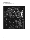
As a reference design, the ADS8402/ADS8412EVM contains the essential
circuitry to showcase the analog-to-digital converter. This essential circuitry
includes the input amplifier, reference circuit, and buffers. The EVM analog
input circuit is optimized for 100-kHz sine wave. Therefore, users may need
to adjust the resistor and capacitor values of the A/D input circuit. In ac-type
applications where signal distortion is a concern, polypropylene capacitors
should be used in the signal path.
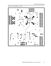
5.2 As a Prototype Board
As a prototype board, the buffer circuit consists of resistor pads for configuring
the input as either single-ended or differential input. The input circuit can be
modified to accommodate user prototype needs, whether it be evaluating
another differential amplifier or limiting noise for best performance. The
analog, power, and digital connectors can be made to plug into a standard
0.1 in. breadboard or cables made up to interface directly to an FPGA or
processor.
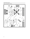
5.3 As a Software Test Platform
As a software test platform, connectors P1, P2, and P3, plug into the parallel
interface connectors of the 5-6K interface card. The 5-6K interface card sits
on the C5000 and C6000 digital signal processor starter kit (DSK). The
ADS8402/ADS8412EVM is then mapped into the processor’s memory space.
This card also provides an area for signal conditioning. This area can be used
to install application circuit(s) for digitization by the ADS8402/ADS8412
analog-to-digital converter. See the 5-6K interface card user’s guide
(SLAU104) for more information.
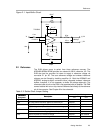
The ADS8402/ADS8412EVM provides a simple platform for interfacing to the
converter. The EVM provides standard 0.1-in. headers and sockets to wire into
prototype boards. The user only needs to provide three address lines (A2, A1,
A0) and address valid line (DC_CS) to connector P2. To choose which address
combinations generates RD, CONVST, and RESET, set jumpers as shown in
Table 4-2. The recall chip select (CS) signal is not memory-mapped or tied to
P2; therefore, it must be controlled via a general purpose pin or shorted to
ground at J3 pin 1. If address decoding is not required, the EVM provides direct
access to converter data bus via P3 and control via J3.