


3-1
Digital Interface
Digital Interface
The ADS8402/ADS8412 EVM is designed for easy interfacing to multiple
platforms. Samtec part numbers SSW-110-22-F-D-VS-K and
TSM-110-01-T-DV-P provide a convenient dual row header/socket
combination at P2 and P3. Consult Samtec at www.samtec.com or
1-800-SAMTEC-9 for a variety of mating connector options.
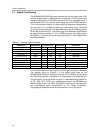
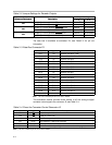
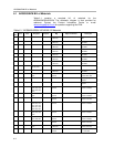
Table 3-1.Pinout for Parallel Control Connector P2
Connector.Pin Signal Description
P2.1 DC_CS Daughter card board select pin
P2.3
P2.5
P2.7 A0 Address line from processor
P2.9 A1 Address line from processor
P2.11 A2 Address line from processor
P2.13
P2.15
P2.17
P2.19 INTc Set jumper W3 to select BUSY or inverted signal
to be applied to this pin.
Note: All even numbered pins of P2 are tied to DGND.
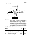
The read (RD), conversion start (CONVST), and reset (RESET) signals to the
converter can be assigned to two different addresses in memory via jumper
settings. This allows for the stacking of up to two ADS8402EVMs and/or
ADS8412EVMs into processor memory. See Table 3-2 for jumper settings.
Note, the evaluation module does not allow the chip select (CS) line of the
converter to be assigned to different memory locations. It is therefore
suggested the CS line be grounded or wired to an appropriate signal of the
processor.
Chapter 3