3-2
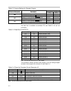
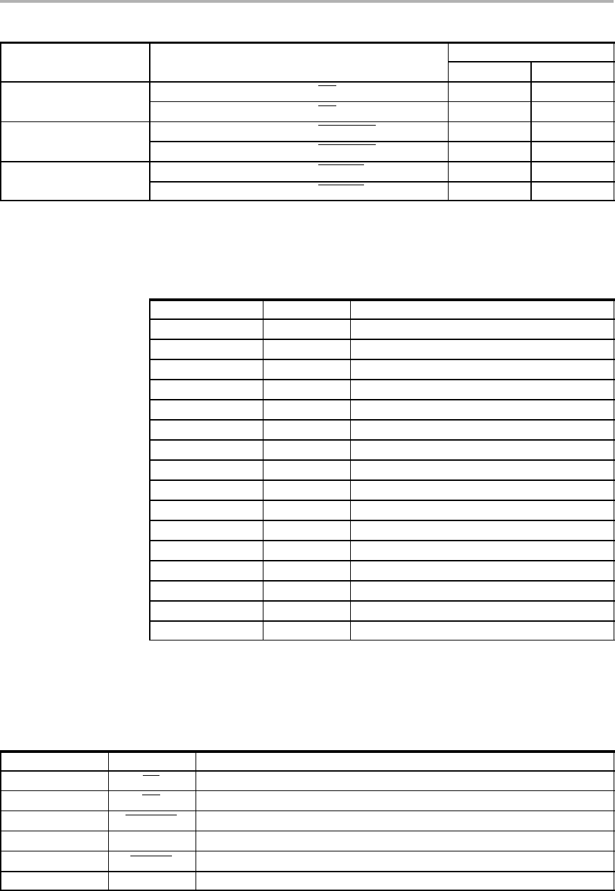
Table 3-2.Jumper Settings for Decoder Outputs
Reference Designator
Description
Jumper Settings
Reference Designator Description
1-2 2-3
W2
Set A[2..0] = 0x1 to generate RD pulse Installed
†
Not installed
W2
Set A[2..0] = 0x2 to generate RD pulse Not installed Installed
W5
Set A[2..0] = 0x3 to generate CONVST pulse Installed
†
Not installed
W5
Set A[2..0] = 0x4 to generate CONVST pulse Not installed Installed
W4
Set A[2..0] = 0x5 to generate RESET pulse Installed
†
Not installed
W4
Set A[2..0] = 0x6 to generate RESET pulse Not installed Installed
†
Factory set condition
The data bus is available at connector P3, see Table 3-3 for pin out
information.
Table 3-3.Data Bus Connector P3
Connector.Pin Signal Description
P3.1 D0 Buffered Data Bit 0 (LSB)
P3.3 D1 Buffered Data Bit 1
P3.5 D2 Buffered Data Bit 2
P3.7 D3 Buffered Data Bit 3
P3.9 D4 Buffered Data Bit 4
P3.11 D5 Buffered Data Bit 5
P3.13 D6 Buffered Data Bit 6
P3.15 D7 Buffered Data Bit 7
P3.17 D8 Buffered Data Bit 8
P3.19 D9 Buffered Data Bit 9
P3.21 D10 Buffered Data Bit 10
P3.23 D11 Buffered Data Bit 11
P3.25 D12 Buffered Data Bit 12
P3.27 D13 Buffered Data Bit 13
P3.29 D14 Buffered Data Bit 14
P3.31 D15 Buffered Data Bit 15
Note: All even numbered pins of P3 are tied to DGND.
This evaluation module provides direct access to all the analog-to-digital
converter control signals via connector J3, see Table 3-4.
Table 3-4.Pinout for Converter Control Connector J3
Connector.Pin Signal Description
J3.1 CS Chip select pin. Active low
J3.3 RD Read pin. Active low
J3.5 CONVST Convert start pin. Active low
J3.7 BYTE Byte mode pin. Used for 8-bit buses.
J3.9 RESET Reset pin. Active low.
J3.11 BUSY Converter status output. High when a conversion is in progress.
Note: All even numbered pins of J3 are tied to DGND.


