CALIBRATION AND REPAIR
17
OFFSET ADJUSTMENT
The SR560's front-panel offset adjustment
provides an easy way for the user to null the
amplifier's DC offset. Use the COUPLING
pushbutton to light the GND LED. Now,
regardless of the SOURCE setting, the input
to the amplifier is grounded internally.
Insert a small screwdriver through the front-
panel OFFSET hole and adjust the offset
potentiometer until the DC offset of the
amplifier (e.g. as viewed on a DVM) is zero.
Finally, return to the desired coupling.
CALIBRATION
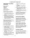
There are four pots, which are used to
calibrate the instrument. The pots adjust
the front-end CMRR (Common Mode
Rejection Ratio) and offset. These pots are
located close to the front of the instrument,
and may be accessed by removing the
bottom cover.
These pots should be adjusted to optimize
the CMRR or null the offset when the front-
end FET is replaced. Two of the pots adjust
the CMRR and offset when the front-end
gain is x10, and two adjust the CMRR and
offset when the front-end gain is x2. The
x10 gain pots must be set first, followed by
the x2 gain pots.
First, the front panel offset pot must be set
to zero:
• Adjust front panel Offset pot to read
0 VDC on pin 14, U407.
Next adjust the offset and CMRR for the
case where the front-end gain is x10. View
the amplifier output on a scope and perform
the following adjustments:
• Couple = GND, Gain = 5 k, LOW
NOISE: adjust P103 to null DC and
output.
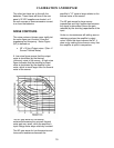
Now use a function generator as the source
of a common mode signal:
• Apply 1 kHz 1 Vpp sine to both the A
and B inputs.
• Couple = DC, source = A - B: adjust
P102 to null sine wave output.
Now adjust the offset and CMRR for the
case where the front-end gain is x2. View
the amplifier output on a scope and perform
the following adjustments:
• Couple = GND (remove signal from
A and B inputs), Gain = 5 k, HIGH
DR: adjust P104 to null DC and
output.
• Apply 1 kHz 1 Vpp sine to both the A
and B inputs.
• Couple = DC, source = A - B: adjust
P101 to null sine wave output.
NOTE
: In the above procedures, the gain of
the front-end (x10 or x2) is determined by
the selection of LOW NOISE or HIGH
DYNAMIC RESERVE.
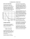
FRONT END REPLACEMENT
The most commonly damaged component
is the front-end FET (U106, National
Semiconductor Corp. P/N NPD5564). It is
located in an 8-pin DIP socket behind the
relays near the input BNCs. If the
instrument exhibits a constant overload,
excessive drift or noise, or large input bias
currents, it is likely that this component has
been damaged.
When replacing the FET, be certain that all
eight pins are inserted into the socket, and
observe the orientation of pin #1. After
replacement adjust the CMRR and offset
per the calibration procedure. More severely
damaged front-ends may require
replacement of op-amp, U102.


