


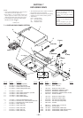

– 79 –
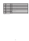
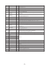
Pin No. Pin Name I/O Function
63
64
65
66
67
68
69
70
71
72
73
74
75
76
77
78
79
80
81
82
83
84
85
86
87,88
89
90
91
92
93 to 95
96
97
98
99
100
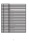
NC
GND
SDA
MNT3 (SLOCK)
WR PWR
PROTECT
REFLECT
LDON
SENS
NMT1 (SHOCK)
DIG-RST
MNT2 (XBUSY)
XLATCH
MOD
LIMIT-IN
MNT0 (FOK)
SCL
SCTX
CLKSET0
CLKSET1
LED0
LED1
NC
OPT SEL
NC
SOURCE
NC
TIMER
NC
KEY 3 to KEY 1
AVSS
KEY0
VREF
+3.3V
MONO/ST
O
—
I/O
I
O
I
I
O
I
I
O
I
O
O
I
I
O
O
I
I
O
O
O
O
O
I
O
I
O
I
—
I
—
—
I
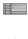
Not used (Fixed at “L”)
Ground
Data signal input/output pin with the backup memory
In the state of spindle srvo lock from the CXD2564R
Write power ON/OFF output
Recording-protection claw detection input from the protection detection switch
Protect: “H”
Disk reflection rate detection input from the reflect detection switch
Disk with low reflection rate: “H”
Laser ON/OFF control output “H”: Laser ON
Internal status (SENSE) input from the CXD2654R
Track jump signal input from the CXD2654R
Digital rest signal output to the CXD2654R and motor driver Reset: “L”
In the state of executive command from the CXD2654R
Latch signal output to the serial bus
Laser modulation switching signal output
Detection input from the limit switch
Sled limit-In: “L”
Focus OK signal input from the CXD26504R
“H” is input when focus is on
Clock signal output to the backup memory
Writing data transmission timing output to the CXD2654R
Shared with the magnetic head ON/OFF output
Clock destination select pin US, Canadian: “L”, Except US, Canadian :“H”
Clock destination select pin US, Canadian: “H”, Except US, Canadian :“L”
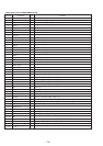
Not used
Input source change input (A/D input)
Not used
Timer mode change input (A/D input)
Not used
Key input pin (A/D input)
Ground (Analog)
Key input pin (A/D input)
A/D reference voltage (Fixed at “H”)
+3.3V power supply
Monaural, stereo change input Monaural: “H”