


– 49 – – 50 –
MDS-JE520
THIS NOTE IS COMMON FOR PRINTED WIRING
BOARDS AND SCHEMATIC DIAGRAMS.
(In addition to this, the necessary note is printed
in each block.)
For schematic diagrams.
Note:
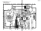
• All capacitors are in µF unless otherwise noted. pF: µµF
50 WV or less are not indicated except for electrolytics
and tantalums.
• All resistors are in Ω and
1
/
4
W or less unless otherwise
specified.
•
¢
: internal component.
• C : panel designation.
For printed wiring boards.
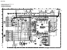
Note:
• X : parts extracted from the component side.
• Y : parts extracted from the conductor side.
•
p : parts mounted on the conductor side.
•
®
: Through hole.
• b : Pattern from the side which enables seeing.
(The other layers' patterns are not indicated.)
• U : B+ Line.
• V : B– Line.
• H : adjustment for repair.
• Voltages and waveforms are dc with respect to ground in
playback mode.
no mark : STOP
( ) : Play the test disc (TDYS-1)
< > : REC
∗
: can not be measured.
• Voltages are taken with a VOM (Input impedance 10 MΩ).
Voltage variations may be noted due to normal produc-
tion tolerances.
• Waveforms are taken with a oscilloscope.
Voltage variations may be noted due to normal produc-
tion tolerances.
• Circled numbers refer to waveforms.
• Signal path.
E : PB
j : REC
p : PB (Digital out)
l : PB (Digital in)
• Abbreviation
CND : Canadian model.
SP : Singapore model.
Note:
The components identi-
fied by mark ! or dotted
line with mark ! are criti-
cal for safety.
Replace only with part
number specified.
Note:
Les composants identifiés par
une marque ! sont critiques
pour la sécurité.
Ne les remplacer que par une
piéce portant le numéro
spécifié.
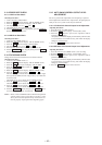
Caution:
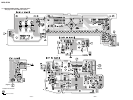
Pattern face side: Parts on the pattern face side seen from the
(Side B) pattern face are indicated.
Parts face side: Parts on the parts face side seen from the
(Side A) parts face are indicated.
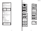
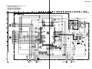
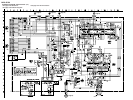
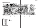
WAVEFORMS
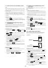
• BD BOARD (1/2)
IC121 !§ (OSCI)
IC101 8, 9 (E, F) (PLAY mode)
IC121 @• (XBCK)
1
2
3
4
5
6
IC121 @ª (FS256)
7
IC121 (º (FS4)
8
IC101 1, 2 (I, J) (PLAY mode)
IC121 @¶ (LRCK)
IC101 4 (A) (PLAY mode)
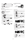
• MAIN BOARD
IC321 !¡ (BCK1), @§ (BCK)
IC321 0 (LRCK1), @• (LRCK)
1
2
3
IC501 !£ (XOUT)
IC321 !∞ (MCK1), @™ (256CK)
4
IC321 @∞ (512FS)
5
IC321 #∞ (XOUT)
6
• DISPLAY BOARD
1
IC771 ^§ (OSCO)
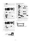
• BD BOARD (2/2)
0.46Vp-p
3.1Vp-p
22.581MHz
3.2Vp-p
44.1kHz
3.8Vp-p
2.822MHz
3.8Vp-p
11.29MHz
3.2Vp-p
176.4kHz
3.2Vp-p
7MHz
3.3Vp-p
44.1kHz
5.2Vp-p
2.822MHz
5.6Vp-p
11.29MHz
3.4Vp-p
22.581MHz
5Vp-p
22.58MHz
3.9Vp-p
2.4MHz
0.1Vp-p
0.06Vp-p