


– 78 –
1, 2
3
4
5
6
7
8
9
10
11
12
13
14
15
16
17
18
19
20
21, 22
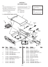
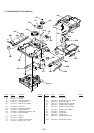
23 to 30
31
32
33
34
35
36
37
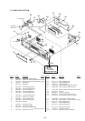
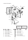
38 to 45
46
47
48
49
50
51
52
53
54
55
56
57, 58
59
60
61
62
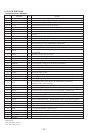
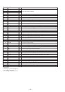
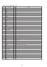
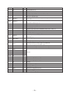
Pin No. Pin Name I/O Function
• IC501 System Control (M30610MCA-251FP)
O
O
O
I
I
O
I
—
O
O
I
O
—
I
—
I
I
I
I
I
O
O
I
O
O
O
O
O
O
I
O
O
O
O
I
I
I
I
O
O
O
I
I
O
—
Not used (Fixed at “L”)
C1 error rate voltage output (Fixed at “L”)
AD error rate voltage output (Fixed at “L”)
ADIP sync or subcode Q sync input from CXD2654R
Remote controls
Not used (Fixed at “L”)
Data bus changed input (Fixed at “L”)
Ground
Not used (Fixed at “L”)
Not used (Fixed at “L”)
System rest input
Main clock output (7.0MHz)
Ground
Main clock input (7.0MHz)
+3.3V power supply
(Fixed at “H”)
Digital in sync input
Power down detection input “L”: Power down
Interrupt status input from CXD2654R
JOG dial pulse input from the rotary encoder
Not used
Writing data signal output to the serial bus
Reading data signal input from the serial bus
Clock signal output to the serial bus
Chip select signal output to the display driver
Serial data signal output to the display driver
Not used (Fixed at “L”)
Serial clock signal output to the display driver
Not used
Loading conatrol system select signal input (Fixed at “L”)
Not used (Fixed at “L”)
Reset signal output to the D/A, A/D converter Reset: “L”
DA line out muting output Mute: “L”
Strobe signal output to the power supply circuit Power supply ON: “H”, stand by: “L”
Detection input from the chucking-in switch “L”: Chucking
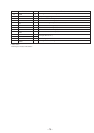
Detection input from the disc detection switch (Fixed at “L”)
Detection input from the loading out switch. Loaded out position: “L”, Others: “H”
Loading motor control input
Loading motor control output
Loading motor voltage control output Low voltage: “H”
Not used (Fixed at “L”)
Detection signal input from the recording position detection switch
Detection signal input from the playback position detection switch
Operation mode output Write: “H”
+3.3V power supply
NC
C1ER
ADER
SQSY
RMC
NC
BYTE
CNVSS
XIN-T
XOUT-T
S.RST
XOUT
VSS
XIN
+3.3V
NMI
DQSY
P.DOWN
XINT
JOG1, JOG0
NC
SWDT
SRDT
SCLK
FLCS
FLDATA
NC
FLCLK
NC
LOADING SEL: L
NC
DA.RST
MUTE
STB
CHACK IN
PACK-IN
PACK-OUT
LDIN
LDOUT
LD-LOW
NC
REC-P
PB-P
REC/PB
+3.3V