Philips Semiconductors ISP1561 Evaluation Board User’s Guide
UM10005_3 © Koninklijke Philips Electronics N.V. 2003. All rights reserved.
User’s Guide Rev. 2.0—April 2003 4 of 20
1. Introduction
The ISP1561 evaluation board is a standard implementation of the ISP1561 in a complete configuration that allows
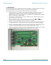
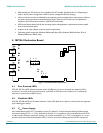
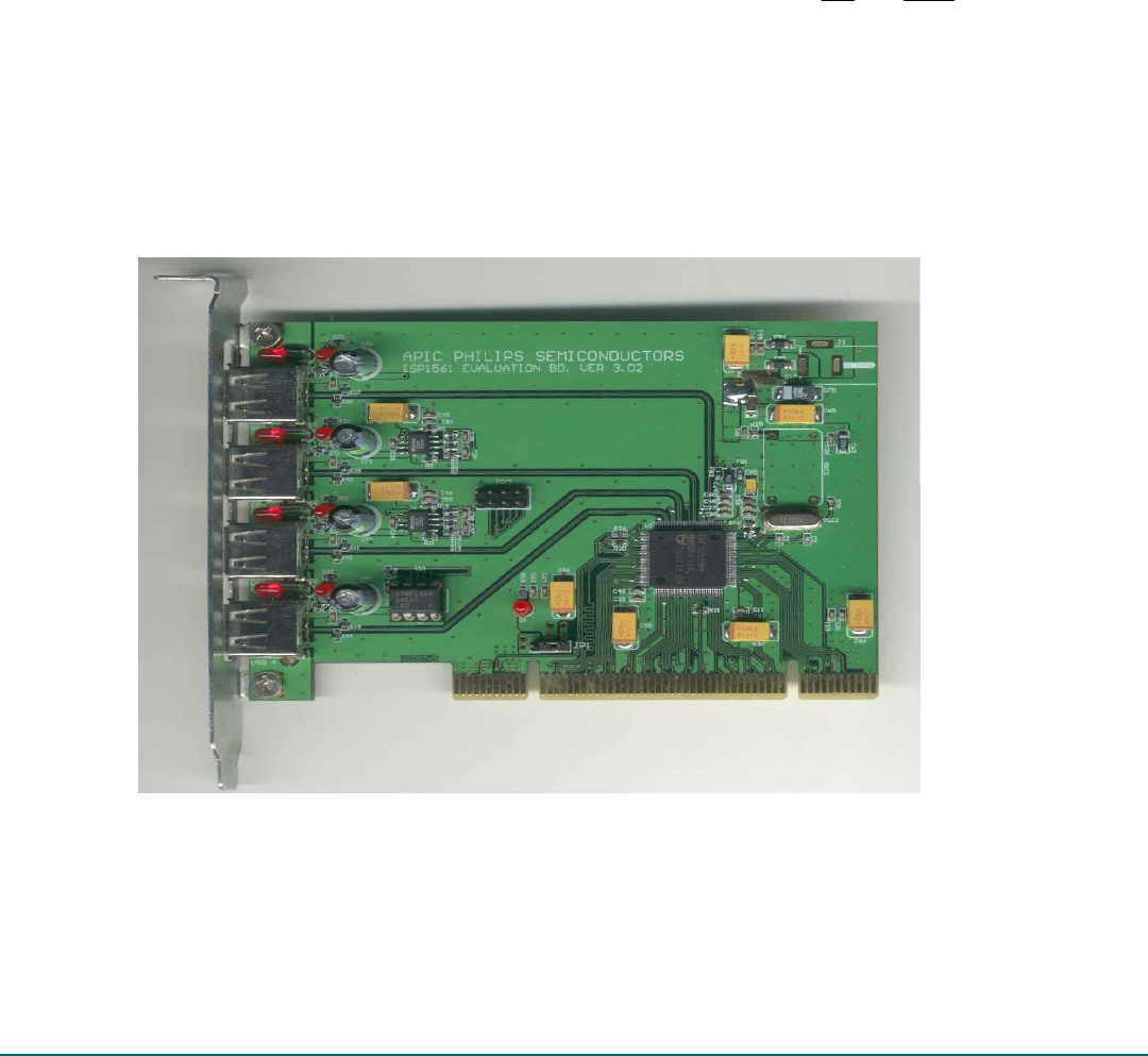
you to exercise all signals and main features. Figure 1-1 shows the ISP1561 evaluation board.
Some of the features that are implemented in the ISP1561 evaluation board are as follows:
• Selection between PCI V
AUX
and PCI V
CC
power supply, with voltage presence indicator. This feature in
combination with the auxiliary +5 V input on J1 allows testing the system wake-up from power
management states, such as S3cold, in which PCI V
CC
is not present. This is intended mainly for testing the
ISP1561 in motherboard or notebook designs.
• Selection between 12 MHz clock (from a crystal) or 48 MHz clock (from a 48 MHz oscillator) input. By
default, 12 MHz crystal is implemented.
• Simple and reliable overcurrent protection scheme that allows testing of the
OCn
and
PWEn
signals.
Alternative solutions (resettable circuit protection devices) can be adopted.
• Port power and GoodLink™ LEDs. These may be omitted in a standard commercial implementation but
are considered useful on the evaluation board for easier understanding of functionality and debugging.
• Connector for testing legacy signals in the case of an on-board solution design. Testing the legacy feature
requires a motherboard with BIOS support for USB or legacy implementation on OHCI.
• Input for an external power supply (J1). This allows complete testing of power management on a standard
mainboard, including the power management modes in which the PCI +5 V is cut off.
Figure 1-1: ISP1561 Evaluation Board


