


1997 Feb 27 5
Philips Semiconductors Product specification
IF amplifier/demodulator for FM radio receivers TDA1597
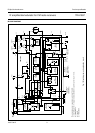
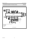
FUNCTIONAL DESCRIPTION
The limiter amplifier has five stages of IF amplification
using balanced differential limiter amplifiers with emitter
follower coupling.
Decoupling of the stages from the supply voltage line and
an internal high-ohmic DC feedback loop gives a very
stable IF performance. The amplifier gain is virtually
independent of changes in temperature.
The FM demodulator is fully balanced and contains two
cross-coupled differential amplifiers.
The quadrature detection of the FM signal is performed by
direct feeding of one differential amplifier from the limiter
amplifier output and the other via an external 90 degrees
phase shifting network. The demodulator has a good
stability and a small zero cross-over shift. The bandwidth
of the demodulator output is restricted by an internal
low-pass filter to approximately 1 MHz. Non-linearities,
which are introduced by demodulation, are compensated
for by the THD compensation circuit. For this reason, the
demodulator resonance circuit (between pins 10 and 11)
must have a loaded Q-factor of 19.
Consequently, there is no need for the demodulator tuned
circuit to be adjusted for minimum distortion. Adjustment
criterion is a symmetrical stop pulse. The control voltage
for the mute attenuator (pin 16) is derived from the values
of the level detector and the detuning detector output
signals. The mute attenuator has a fast attack and a slow
decay, determined by the capacitor connected to pin 16.
The AF signal is fed via the mute attenuator to the output
(pin 4). A weighted control voltage (pin 6) is obtained from
the mute attenuator control voltage via a buffer amplifier
that introduces an additional voltage shift and gain.
The level detector generates a voltage output signal
proportional to the amplitude of the input signal.
The unweighted level detector output signal is available in
the FM-MUTE-ON condition (mode switch).
The open-collector tuning stop output voltages STOP-0
and STOP-1 (pins 15 and 14) are derived from the
detuning and the input signal level. Pins 14 and 15 may be
tied together if only one tuning-stop output is required.
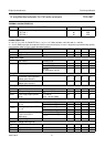
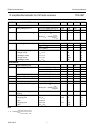
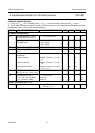
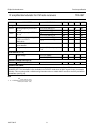
LIMITING VALUES
In accordance with the Absolute Maximum Rating System (IEC 134).
Note
1. Equivalent to discharging a 100 pF capacitor through a 1.5 kΩ series resistor.
SYMBOL PARAMETER CONDITIONS MIN. MAX. UNIT
V
P
supply voltage −0.3 +13 V
V
n
voltage at pins 2, 4, 5, 6, 10, 11 and 16 −0.3 +10 V
voltage at pins 3, 7, 8, 14, 15, 18,
19 and 20
−0.3 V
P
V
V
13
voltage on pin 13 − 6V
I
14, 15
current at pins 14 and 15 − 2mA
P
tot
total power dissipation − 360 mW
T
stg
storage temperature −55 +150 °C
T
amb
operating ambient temperature −40 +85 °C
V
es
electrostatic handling
all pins except pins 5 and 7 note 1 −2000 +2000 V
pin 5 note 1 −2000 +800 V
pin 7 note 1 −2000 +1000 V