


2004 Jan 28 7
Philips Semiconductors Product specification
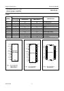
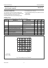
22 W BTL or 2 × 11 W
stereo power amplifier
TDA1519C
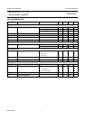
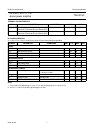
THERMAL CHARACTERISTICS
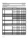
DC CHARACTERISTICS
V
P
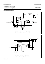
= 14.4 V; T
amb
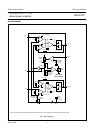
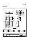
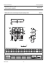
=25°C; measured in circuit of Fig.6; unless otherwise specified.
Notes
1. The circuit is DC adjusted at V
P
= 6 to 17.5 V and AC operating at V
P
= 8.5 to 17.5 V.
2. At V
P
= 17.5 to 30 V, the DC output voltage is ≤0.5V
P
.
SYMBOL PARAMETER CONDITIONS VALUE UNIT
R
th(j-a)
thermal resistance from junction to ambient;
TDA1519C, TDA1519CTH and TDA1519CTD
in free air 40 K/W
R
th(j-c)
thermal resistance from junction to case;
TDA1519C, TDA1519CTH and TDA1519CTD
3 K/W
SYMBOL PARAMETER CONDITIONS MIN. TYP. MAX. UNIT
Supply
V
P
supply voltage note 1 6.0 14.4 17.5 V
I
q(tot)
total quiescent current − 40 80 mA
V
O
DC output voltage note 2 − 6.95 − V
∆V
OO
DC output offset voltage −−250 mV
Mute/standby switch
V
sw(on)
switch-on voltage level 8.5 −−V
V
mute
mute voltage level 3.3 − 6.4 V
V
stb
standby voltage level 0 − 2V
Mute/standby condition
V
o
output voltage mute mode; V
i
= 1 V (maximum);
f
i
=20Hzto15kHz
−−20 mV
∆V
OO
DC output offset voltage mute mode −−250 mV
I
stb
standby current standby mode −−100 µA
I
sw(on)
switch-on current − 12 40 µA