


2004 Jan 28 18
Philips Semiconductors Product specification
22 W BTL or 2 × 11 W
stereo power amplifier
TDA1519C
applied by screen printing, pin transfer or syringe dispensing. The package can be soldered after the adhesive is cured.
Typical dwell time of the leads in the wave ranges from 3 to 4 seconds at 250 °C or 265 °C, depending on solder material
applied, SnPb or Pb-free respectively.
A mildly-activated flux will eliminate the need for removal of corrosive residues in most applications.
MANUAL SOLDERING
Fix the component by first soldering two diagonally-opposite end leads. Use a low voltage (24 V or less) soldering iron
applied to the flat part of the lead. Contact time must be limited to 10 seconds at up to 300 °C. When using a dedicated
tool, all other leads can be soldered in one operation within 2 to 5 seconds between 270 and 320 °C.
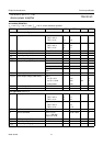
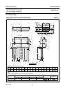
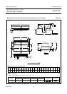
Suitability of IC packages for wave, reflow and dipping soldering methods
Notes
1. For more detailed information on the BGA packages refer to the
“(LF)BGA Application Note
” (AN01026); order a copy
from your Philips Semiconductors sales office.
2. All surface mount (SMD) packages are moisture sensitive. Depending upon the moisture content, the maximum
temperature (with respect to time) and body size of the package, there is a risk that internal or external package
cracks may occur due to vaporization of the moisture in them (the so called popcorn effect). For details, refer to the
Drypack information in the
“Data Handbook IC26; Integrated Circuit Packages; Section: Packing Methods”
.
3. For SDIP packages, the longitudinal axis must be parallel to the transport direction of the printed-circuit board.
4. Hot bar soldering or manual soldering is suitable for PMFP packages.
5. These transparent plastic packages are extremely sensitive to reflow soldering conditions and must on no account
be processed through more than one soldering cycle or subjected to infrared reflow soldering with peak temperature
exceeding 217 °C ± 10 °C measured in the atmosphere of the reflow oven. The package body peak temperature
must be kept as low as possible.
6. These packages are not suitable for wave soldering. On versions with the heatsink on the bottom side, the solder
cannot penetrate between the printed-circuit board and the heatsink. On versions with the heatsink on the top side,
the solder might be deposited on the heatsink surface.
7. If wave soldering is considered, then the package must be placed at a 45° angle to the solder wave direction.
The package footprint must incorporate solder thieves downstream and at the side corners.
MOUNTING PACKAGE
(1)
SOLDERING METHOD
WAVE REFLOW
(2)
DIPPING
Through-hole mount CPGA, HCPGA suitable − suitable
DBS, DIP, HDIP, RDBS, SDIP, SIL suitable
(3)
−−
Through-hole-
surface mount
PMFP
(4)
not suitable not suitable −
Surface mount BGA, HTSSON..T
(5)
, LBGA, LFBGA, SQFP,
SSOP-T
(5)
, TFBGA, USON, VFBGA
not suitable suitable −
DHVQFN, HBCC, HBGA, HLQFP, HSO,
HSOP, HSQFP, HSSON, HTQFP, HTSSOP,
HVQFN, HVSON, SMS
not suitable
(6)
suitable −
PLCC
(7)
, SO, SOJ suitable suitable −
LQFP, QFP, TQFP not recommended
(7)(8)
suitable −
SSOP, TSSOP, VSO, VSSOP not recommended
(9)
suitable −
CWQCCN..L
(11)
, PMFP
(10)
, WQCCN32L
(11)
not suitable not suitable −