


2004 Jan 28 5
Philips Semiconductors Product specification
22 W BTL or 2 × 11 W
stereo power amplifier
TDA1519C
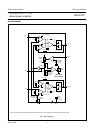
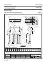
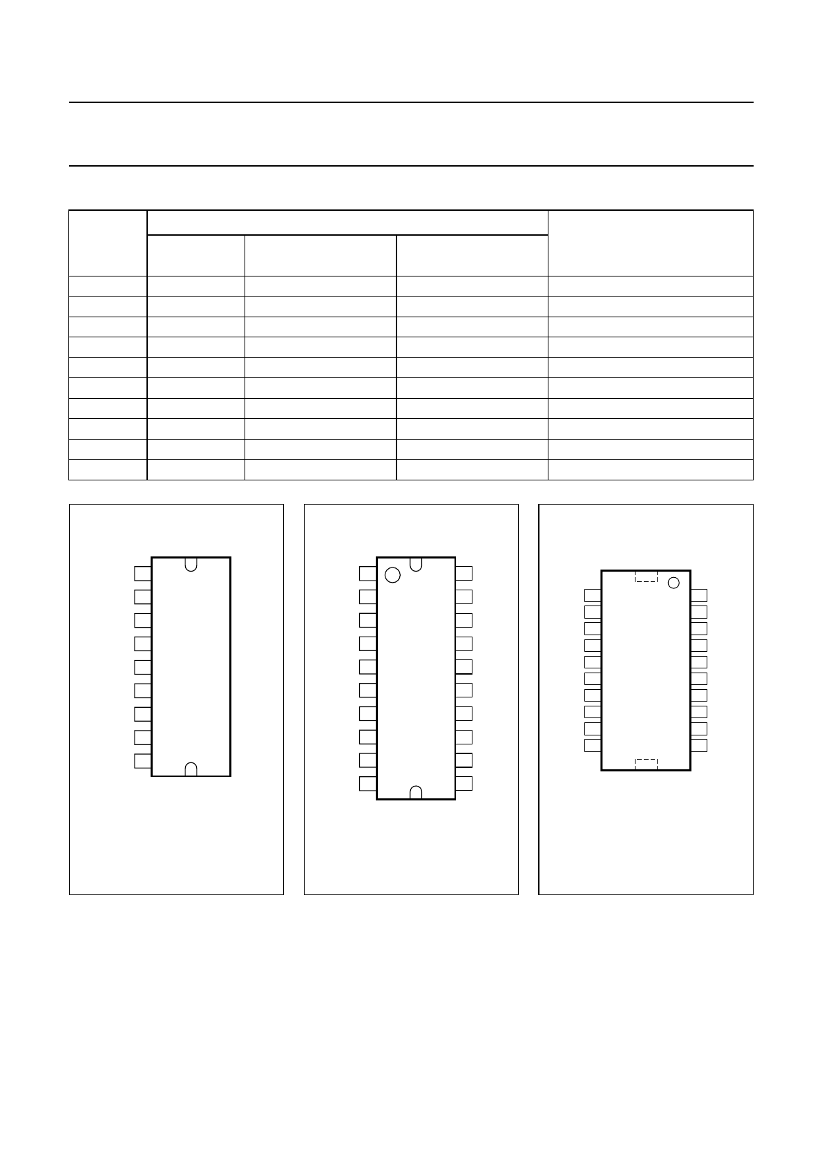
PINNING
SYMBOL
PIN
DESCRIPTION
TDA1519C;
TDA1519CSP
TDA1519CTD TDA1519CTH
NINV 1 19 19 non-inverting input
GND1 2 20 20 ground 1 (signal)
RR 3 1 1 supply voltage ripple rejection
OUT1 4 3 3 output 1
GND2 5 5 5 ground 2 (substrate)
OUT2 6 8 8 output 2
V
P
7 10 10 positive supply voltage
M/SS 8 11 11 mute/standby switch input
INV 9 12 12 inverting input
n.c. − 2, 4, 6, 7, 9 and 13 to 18 2, 4, 6, 7, 9 and 13 to 18 not connected
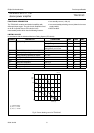
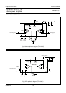
Fig.2 Pin configuration
TDA1519C and
TDA1519CSP.
h
alfpage
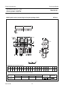
NINV
GND1
RR
OUT1
GND2
OUT2
V
P
M/SS
INV
1
2
3
4
5
6
7
8
9
TDA1519C
TDA1519CSP
MGR561
f
page
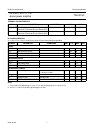
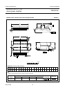
RR
n.c.
OUT1
n.c.
GND2
n.c.
n.c.
OUT2
n.c.
V
P
GND1
NINV
n.c.
n.c.
n.c.
n.c.
n.c.
n.c.
INV
M/SS
1
2
3
4
5
6
7
8
9
10
11
12
20
19
18
17
16
15
14
13
TDA1519CTD
MGL937
Fig.3 Pin configuration
TDA1519CTD.
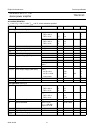
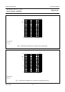
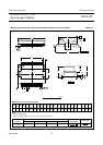
TDA1519CTH
GND1 RR
NINV n.c.
n.c. OUT1
n.c. n.c.
n.c. GND2
n.c. n.c.
n.c. n.c.
n.c. OUT2
INV n.c.
M/SS V
P
001aaa348
20
19
18
17
16
15
14
13
12
11
9
10
7
8
5
6
3
4
1
2
Fig.4 Pin configuration
TDA1519CTH.