2000 Nov 15 2
Philips Semiconductors Preliminary specification
UHF amplifier module BGY280
FEATURES
• Dual band GSM amplifier
• 3.6 V nominal supply voltage
• 33.5 dBm output power for GSM1800
• 35.5 dBm output power for GSM900
• Easy output power control by DC voltage.
• Internal input and output matching.
APPLICATIONS
• Digital cellular radio systems with Time Division Multiple
Access (TDMA) operation (GSM systems) in two
frequency bands: 880 to 915 MHz and
1710 to 1785 MHz.
DESCRIPTION
The BGY280 is a power amplifier module in a SOT559A
leadless package with a plastic cap. The dimensions are
13.75 x 11 x 1.7 mm. The module consists of two
separated line-ups. One for GSM900 and one for
GSM1800. Internal power control, input and output
matching.
PINNING - SOT559A
PIN DESCRIPTION
1,2,3,6,9,10,11,14 Ground
4 RF output 2 (1800 MHz)
5V
S2
(1800 MHz)
7V
S1
(900 MHz)
8 RF output 1 (900 MHz)
12 RF input 1 (900 MHz)
13 V
C1
(900 MHz)
15 V
C2
(1800 MHz)
16 RF input 2 (1800 MHz)
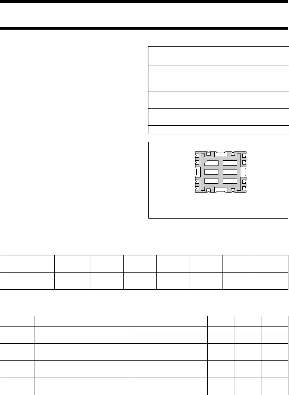
Fig.1 Simplified outline
Bottom view
8
7
5
6
4
12
13
15
14
16
123
11 10 9
MBL031
QUICK REFERENCE DATA
RF performance at T
mb
=25°C.
LIMITING VALUES
In accordance with the Absolute Maximum Rating System (IEC 134).
MODE OF
OPERATION
f
(MHz)
V
S
(V)
V
C
(V)
P
L
(dBm)
G
p
(dB)
η
(%)
Z
S
, Z
L
(Ω)
Pulsed; δ =2:8
880 to 915 3.6 ≤2.2 typ. 35.5 typ. 35.5 47 50
1710 to 1785 3.6 ≤2.2 typ. 33.5 typ. 33.5 40 50
SYMBOL PARAMETER CONDITIONS MIN. MAX. UNIT
V
S1
, V
S2
DC supply voltage
V
C1,2
=0; RF
IN
=off − 7V
V
C1,2
> 0.5 V; RF
IN
=on − 5.5 V
V
C1
, V
C2
DC control voltage − 3V
P
D1
, P
D2
input drive power − 10 mW
P
L1
load power 1 − 4W
P
L2
load power 2 − 3W
T
stg
storage temperature −40 +100 °C
T
mb
operating mounting base temperature −30 +100 °C


