


Philips Semiconductors Application note
AN1651Using the NE/SA5234 amplifier
1991 Oct
7
(EQ. 8.)
ƪ
(0.163x10
* 3
)
2
)
ǒ
4KT @ 100 @ 10,000
Ǹ
Ǔ
2
Ǹ
ƫ
@ 10
+ 1.6mV
(EQ. 9.)
K
+
Boltzman
Ȁ
sConstant
+
T
+
300
o
K ; BW
+
10kHz
1.38x10
*
23
Joule
DegKelvin
The amplified output signal = 1V
RMS
(EQ. 10.)
Sń N + 20 log
10
ǒ
1
1.6x10
* 3
Ǔ
+ 56dB
Note that there is no effect from the second-stage thermally
generated resistor noise due to the dominating effect of the
first-stage amplified noise being much greater than the input noise of
the second-stage. In addition the equivalent noise resistance of the
second-stage is essentially the output resistance of the first-stage
plus any series resistance used in coupling the two. This is the
parallel combination of source resistance with input terminating or
biasing resistance.
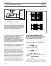
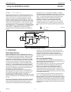
VII. LOW HARMONIC DISTORTION
The NE/SA5234 is extremely well adapted to reducing harmonic
distortion as it relates to signal level and head room in audio and
instrumentation circuits. Its unique internal design limits overdrive
induced distortion to a level much below that experienced with other
low voltage devices. As will be shown, the device is capable of
operating over a wide supply range without causing the typical
clipping distortion prevalent in companion operational amplifiers of
this class.
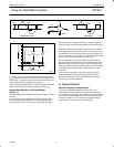
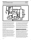
A series of tests are shown to allow you to see just how resistant
this device is to generating clipping distortion. Two different gain
configurations were chosen to demonstrate this particular feature:
unity gain non-inverting and 40dB non-inverting. The test set-up
was as shown in Figure 9. The Harmonic Distortion analyzer used
to make the measurements was a Storage Technology ST1700.
The test frequency is 1kHz. For single supply operation, as
previously covered, the amplifier should be biased to half the supply
voltage to minimize distortion. Operation with dual supplies is
simpler from a parts count standpoint as isolation capacitors are not
required. Also the time constants associated with charging and
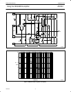
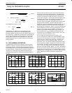
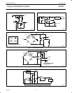
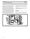
discharging these is eliminated . Figure 10a,b and c shows the total
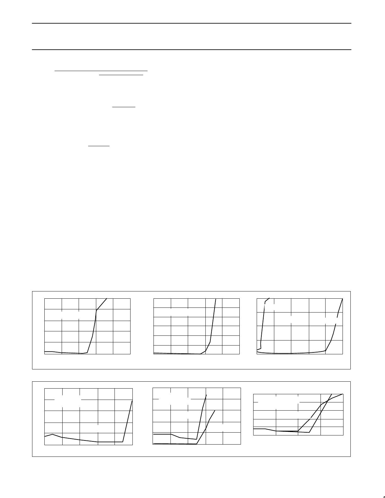
harmonic distortion in percent versus input voltage level at 1kHz in
V
RMS
for a non-inverting, unity gain NE5234. The load on the
amplifier output is 10kΩ. Beginning with a supply voltage of 1.8V
and an input level of 0.1V
RMS
, distortion is well below 0.2% ad
remains there up to an input level just over 0.5V
RMS
(1.4V
P-P
) and
increases to 0.4% for for 0.6V
RMS
(1.7V
P-P
).
For a 2V supply, the input levels increase to 0.65V
RMS
and
0.7V
RMS
, respectively for similar levels of distortion. With a supply
voltage of 3.0V the input may be increased to 1V
RMS
before THD
rises to 0.2% and 1.1V
RMS
for only 0.8% THD. Operation with a
600Ω load will only raise the THD figures slightly . By way of
comparison, Figure 10c shows the greatly reduced dynamic range
experienced when an LM324 is plugged into the test socket in place
of the NE5234. Note that The THD is completely off scale for the
case of 1.8 and 2.0V supply, then is barely usable for the low level
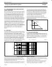
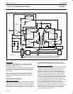
end of the 3.0V supply example. Figure 11a, b, and c demonstrates
the effect on harmonic distortion when closed loop gain is increased
to 40dB in the non-inverting mode. It is evident that little increase in
THD levels result. The graphs for the 2.0 and 3.0V supply case also
include additional information on the effect of a 600Ω load on
distortion.
UNITY GAIN
3
0
0.1
V
1.0
UNITY GAIN
3
0
0.1
V
1.1
a. b.
LM324
NE5234
UNITY GAIN
0.8
0
0.1
V
1.1
c.
SL00638
V
CC
= 1.8V
V
CC
= 2.0V
V
CC
= 3.0V
Figure 10. THD vs Supply Voltage for 1V
RMS
Output
R
L
= 600Ω
R
L
= 10kΩ
3
P
0
0.1
V 0.9
THD for V
CC
= 1.8V
-R
L
= 10k/600Ω
2.5
0
0.1
V 1.1
V
CC
= 2V
R
L
= 10k/600Ω
R
L
= 600Ω
R
L
= 10kΩ
c.b.
R
L
= 10kΩ
V
CC
= 3.0V
GAIN = 40dB
2
0
0.1
V 1.1
a.
SL00639
Figure 11. THD vs Load