


CCT-55-V; DC VOLTAGE INTEGRATOR
ELECTRICAL FEATURES
INPUT
OUTPUT
FREQUENCY : Pulses per second 0 to 10,000 (12 selectable ranges)
Pulses per hour 0 to 8,790 (13 selectable ranges)
TYPE OF PULSES : Voltage 24 Vdc @ 20 mA maximum
Sink Current 100 mA. (24 Vdc external power supply)
PULSE WIDTH 100 ms; 50 % of the full cycle or
variable with frequency ratio
ACCURACY ≤ 0.2 % FS
RESPONSE TIME ≤ 250 ms
GALVANIC ISOLATION Input, Output and Power Supply are all isolated
to 2 kVeff
.
50 Hz/1 m.
GENERAL SPECIFICATIONS
STORAGE TEMPERATURE -30° to +80°C
OPERATING TEMPERATURE -10° to +60°C
TEMPERATURE COEFFICIENT ≤ 0.015 %/°C
STANDARD POWER SUPPLY 115 Vac (±10%) 50/60 Hz
POWER CONSUMPTION ≤ 1.5 VA
TEST VOLTAGE 4 kVeff. 50 Hz/1m.
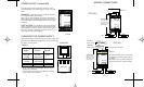
OFFSET ADJUST
Solder pad 1 if closed : Adjust the low range level of the output (Offset positive coarse).
Solder pad 2 if closed : Adjust the low range level of the output (Offset negative coarse).
Jumper A if closed : Adjust the low range level of the output (Offset negative fine).
AMPLIFIER GAIN
Jumper B if closed : Gain at maximum level
Jumper C if closed : Gain at medium level.
Jumpers B and C opened : Gain at minimum level.
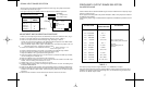
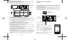
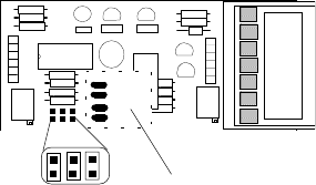
SIGNAL INPUT, module ME
OVERVIEW
P1 :Output zero adjustment.
P2 :Gain amplifier adjustment.
B
2
1
C
A
FIG.7
Solder pads on solder side
P2P1
This module together with the "MP" input board, performs all the input signal conditioning (see
Fig. 2). This module contains the trimmers and jumpers for the amplifier gain and the low level
output (offset).
The signal input connections are made at Terminals 3, 4, 5 and 6.
Each model may use some of these terminals, see the Connections Section.
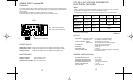
Table 4 indicates all the standard available ranges for the CCT-55-V and its electrical
specifications. The position of the jumpers are indicated in Fig. 8.
For different signal ranges, contact the engineering department for more information.
Reference AB CDE
Range 0 to 100 mV 0 to 1 V 0 to 10 V 0 to 100 V 0 to 650 V
Min. input span * 10 mV 0.1 V 1 V 10 V 100 V
Impedance 100 KΩ 100 KΩ 1 MΩ
Overvoltage 25 V 75 V 1,000 V
*
The minimum input span is the minimum difference between the maximum and minimum
input for a full scale output.
TABLE 4
8
9