


TFA9810_3 © NXP B.V. 2008. All rights reserved.
Product data sheet Rev. 03 — 20 February 2008 4 of 29
NXP Semiconductors
TFA9810
Audio amplifier 2 x 12 W
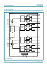
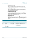
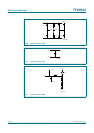
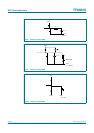
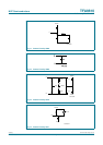
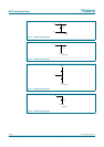
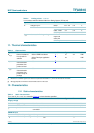
7. Pinning information
7.1 Pinning
The SO32 package has four corner leads. These leads (1, 16, 17, and 32) are internally
connected to the die pad and must be connected to V
SSA
in the application. Together with
the applied copper area on the Printed Circuit Board (PCB) these leads determine the
ambient temperature, which affects the thermal resistance of the junction.
7.2 Pin description
Fig 2. Pin configuration
TFA9810
SO32
V
SSD(HW)
V
SSD(HW)
IN1P STAB1
IN1N V
SSP1
V
DDA1
BOOT1N
V
SSA1
OUT1N
SO/OL BOOT1P
ENABLE OUT1P
CDELAY V
DDP1
n.c. V
DDP2
DIAG OUT2P
TEST BOOT2P
V
SSA2
OUT2N
V
DDA2
BOOT2N
IN2N V
SSP2
IN2P STAB2
V
SSD(HW)
V
SSD(HW
)
010aaa017
1
2
3
4
5
6
7
8
9
10
11
12
13
14
15
16
18
17
20
19
22
21
24
23
26
25
32
31
30
29
28
27
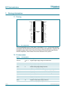
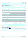
Table 3. Pin description
Symbol Pin Description
V
SSD(HW)
1, 16, 17,
32
Negative digital supply voltage and handle wafer
IN1P 2 Positive input comparator channel 1
IN1N 3 Negative input comparator channel 1
V
DDA1
4 Positive analog supply voltage channel 1
V
SSA1
5 Negative analog supply voltage channel 1
SO/OL 6 SO/OL input enables self-oscillating / open-loop configuration
ENABLE 7 Enable input to switch between SLEEP and OPERATING
CDELAY 8 CDELAY input determines the switch on/off timing
n.c. 9 Not connected
DIAG 10 Diagnostic output; open drain
TEST 11 Test signal input; for testing purposes only
V
SSA2
12 Negative analog supply voltage channel 2
V
DDA2
13 Positive analog supply voltage channel 2