


MAX9777/MAX9778
Stereo 3W Audio Power Amplifiers with
Headphone Drive and Input Mux
2
______________________________________________________________________________________________________________________________________________________________________________
AABBSSOOLLUUTTEE MMAAXXIIMMUUMM RRAATTIINNGGSS
Stresses beyond those listed under “Absolute Maximum Ratings” may cause permanent damage to the device. These are stress ratings only, and functional
operation of the device at these or any other conditions beyond those indicated in the operational sections of the specifications is not implied. Exposure to
absolute maximum rating conditions for extended periods may affect device reliability.
V
DD
to GND ...........................................................................+6V
PV
DD
to V
DD
.......................................................................±0.3V
PGND to GND.....................................................................±0.3V
All Other Pins to GND.................................-0.3V to (V
DD
+ 0.3V)
Continuous Input Current (into any pin except power-supply
and output pins) ...............................................................±20mA
OUT__ Short Circuit to GND, V
DD
..........................................10s
Short Circuit Between OUT_+ and OUT_- .................Continuous
Continuous Power Dissipation (T
A
= +70°C)
28-Pin TQFN, Multilayer Board
(derate 34.5mW/°C above +70°C)..........................2758.6mW
Operating Temperature Range ...........................-40°C to +85°C
Storage Temperature Range.............................-65°C to +150°C
Junction Temperature......................................................+150°C
Lead Temperature (soldering, 10s).................................+300°C
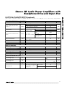
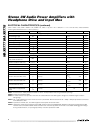
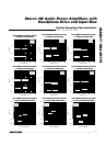
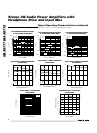
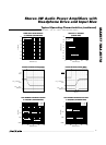
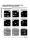
ELECTRICAL CHARACTERISTICS
(V
DD
= PV
DD
= 5.0V, GND = PGND = 0V, V
SHDN
= 5V, C
BIAS
= 1µF, R
IN
= R
F
= 15kΩ, R
L
= ∞. T
A
= T
MIN
to T
MAX
, unless otherwise
noted. Typical values are at T
A
= +25°C.) (Note 1)
PARAMETER SYMBOL CONDITIONS MIN TYP MAX UNITS
Supply Voltage Range V
DD
/PV
DD
Inferred from PSRR test 4.5 5.5 V
BTL mode, HPS = 0V, MAX9777/MAX9778 13 32
Quiescent Supply Current
(I
VDD
+ I
PVDD
)
I
DD
Single-ended mode, HPS = V
DD
718
mA
Shutdown Current I
SHDN
SHDN = GND 10 50 µA
Switching Time t
SW
Gain or input switching 10 µs
C
BIAS
= 1µF 300
Turn-On Time t
ON
C
BIAS
= 0.1µF 30
ms
Thermal Shutdown Threshold +160
o
C
Thermal Shutdown Hysteresis 15
o
C
OUTPUT AMPLIFIERS (SPEAKER MODE, HPS = GND)
Output Offset Voltage V
OS
OUT_+ - OUT_-, A
V
= 1V/V ±4 ±32 mV
V
DD
= 4.5V to 5.5V 75 100
f = 1kHz, V
RIPPLE
= 200mV
P-P
82
Power-Supply Rejection Ratio
(Note 2)
PSRR
f = 20kHz, V
RIPPLE
= 200mV
P-P
70
dB
R
L
= 8Ω 1.4
R
L
= 4Ω 2.6Output Power P
OUT
f
IN
= 1kHz,
THD+N < 1%,
T
A
= +25°C
R
L
= 3Ω 3
W
P
OUT
= 1W, R
L
= 8Ω 0.005
Total Harmonic Distortion Plus
Noise
THD+N
f
IN
= 1kHz, BW =
22Hz to 22kHz
P
OUT
= 2W, R
L
= 4Ω 0.01
%
Signal-to-Noise Ratio SNR R
L
= 8Ω, P
OUT
= 1W, BW = 22Hz to 22kHz 95 dB
Slew Rate SR 1.6 V/µs
Maximum Capacitive Load Drive C
L
No sustained oscillations 1 nF
Crosstalk f
IN
= 10kHz 73 dB
Into shutdown -50
Click/Pop Level K
CP
Peak voltage, A-weighted,
32 samples per second
(Notes 2, 6)
Out of shutdown -65
dBV