


MAX9777/MAX9778
Stereo 3W Audio Power Amplifiers with
Headphone Drive and Input Mux
16
____________________________________________________________________________________________________________________________________________________________________________
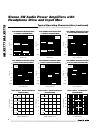
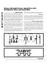
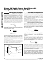
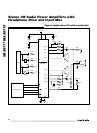
Write Data Format
There are three registers that configure the MAX9777:
the MUTE register, SHDN register, and control register.
In write data mode (R/W = 0), the register address and
data byte follow the device address (Figure 7).
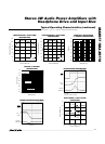
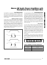
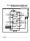
MUTE Register
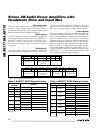
The MUTE register (01hex) is a read/write register that
sets the MUTE status of the device. Bit 3 (MUTEL) of
the MUTE register controls the left channel; bit 4
(MUTER) controls the right channel. A logic-high mutes
the respective channel; a logic-low brings the channel
out of mute.
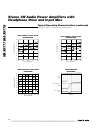
SHDN Register
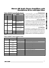
The SHDN register (02hex) is a read/write register that
controls the power-up state of the device. A logic-high
in bit 0 of the SHDN register shuts down the device; a
logic-low turns on the device. A logic-high is required in
bits 2 to 7 to reset all registers to their default settings.
Control Register
The control register (03hex) is a read/write register that
determines the device configuration. Bit 1 (IN1/IN2) con-
trols the input multiplexer, a logic-high selects input 1; a
logic-low selects input 2. Bit 2 (HPS_D) controls the
headphone sensing. A logic-low configures the device in
automatic headphone detection mode. A logic-high dis-
ables the HPS input. Bit 3 (GAINA/B) controls the gain-
select multiplexer. A logic-low selects GAINA. A logic-
high selects GAINB. GAINA/B is ignored when HPS_D =
0. Bit 4 (SPKR/HP) selects the amplifier operating mode
when HPS_D = 1. A logic-high selects speaker mode,
and a logic-low selects headphone mode.
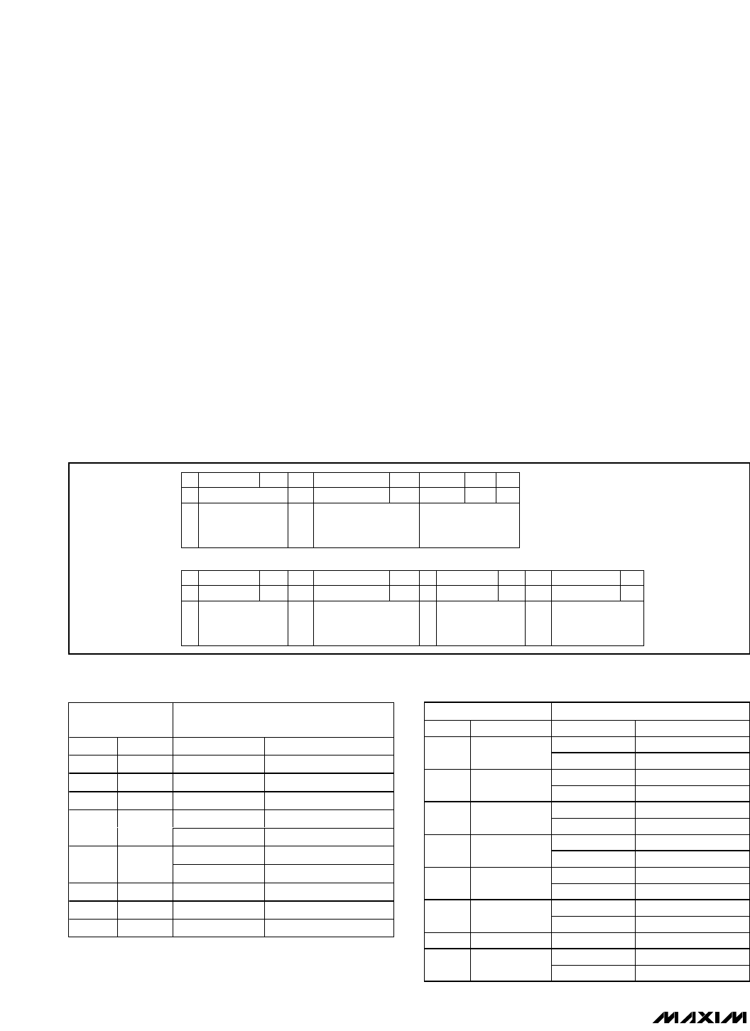
S ADDRESS
7 BITS 8 BITS 8 BITS 1
WR ACK COMMAND ACK DATA ACK P
I
2
C SLAVE ADDRESS.
SELECTS DEVICE.
REGISTER ADDRESS.
SELECTS REGISTER TO BE
WRITTEN TO.
REGISTER DATA
I
2
C SLAVE ADDRESS.
SELECTS DEVICE.
DATA FROM
SELECTED REGISTER
S ADDRESS
7 BITS 8 BITS 8 BITS 1
WR ACK COMMAND ACK DATA P
I
2
C SLAVE ADDRESS.
SELECTS DEVICE.
REGISTER ADDRESS.
SELECTS REGISTER
TO BE READ.
S ADDRESS
7 BITS
WR ACK
Figure 7. Write/Read Data Format Example
REGISTER
ADDRESS
0000 0001
BIT NAME VALUE DESCRIPTION
7 X Don’t Care —
6 X Don’t Care —
5 X Don’t Care —
0* Unmute right channel
4 MUTER
1 Mute right channel
0* Unmute left channel
3 MUTEL
1 Mute left channel
2 X Don’t Care —
1 X Don’t Care —
0 X Don’t Care —
Table 3. MAX9777 MUTE Register Format
*Default state.
REGISTER ADDRESS 0000 0010
BIT NAME VALUE DESCRIPTION
0* —
7 RESET
1 Reset device
0* —
6 RESET
1 Reset device
0* —
5 RESET
1 Reset device
0* —
4 RESET
1 Reset device
0* —
3 RESET
1 Reset device
0* —
2 RESET
1 Reset device
1 X Don’t Care —
0* Normal operation
0 SHDN
1 Shutdown
Table 4. MAX9777 SHDN Register Format
*Default state.