VHF (7610) CIRCUIT DESCRIPTION
5A-4
November 1998
Part No. 001-7600-001
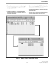
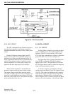
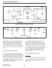
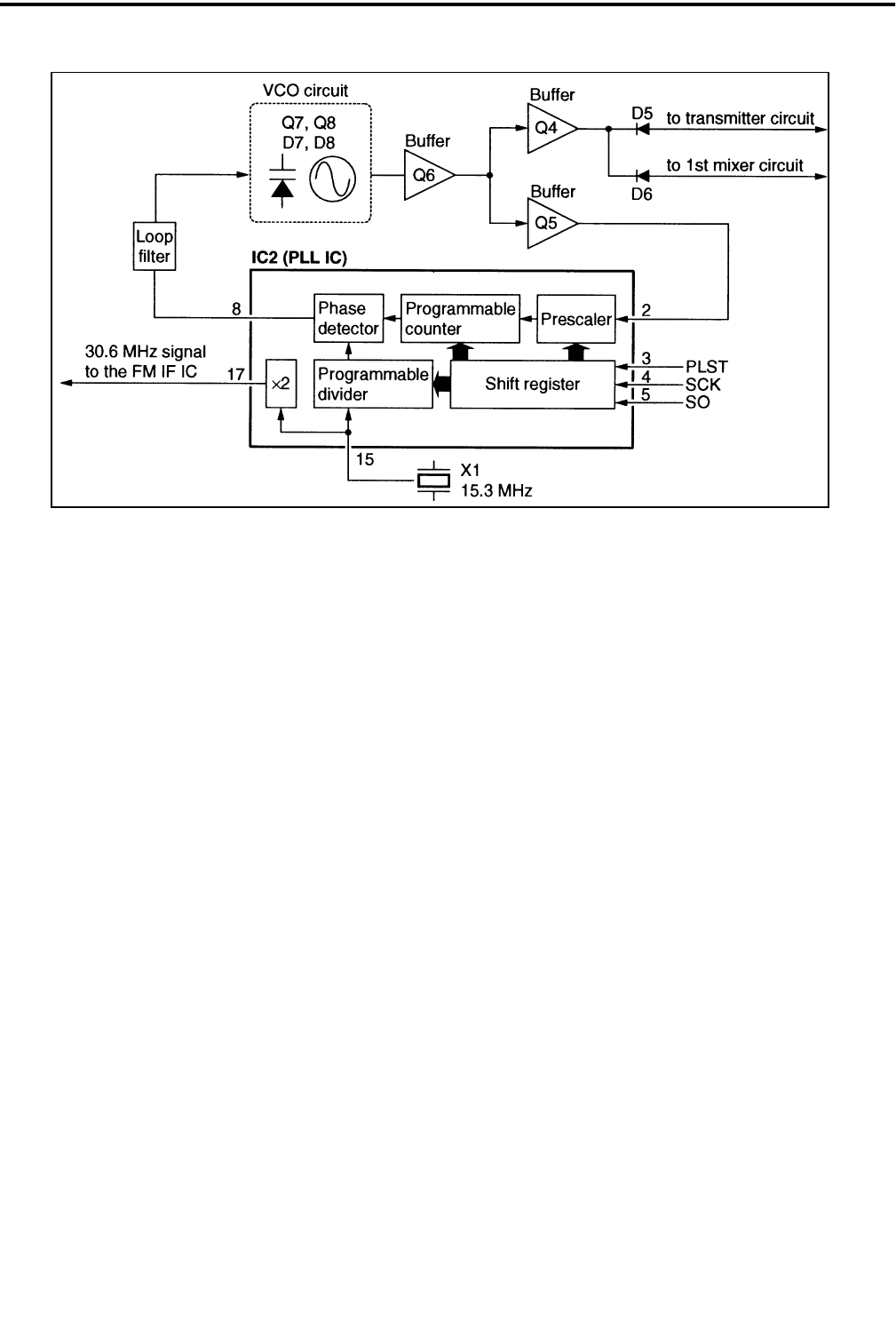
Figure 5-3 PLL Circuit (VHF)
5.2.5 APC CIRCUIT
The APC (Automatic Power Control) circuit pro-
tects the power amplifier from damage caused by a
mismatched antenna load, and provides a stable power
output.
Detector D2 detects forward signals, and D1
detects reverse signals. The combined voltage is at
minimum level when a matched antenna load of 50
ohms is present and then increases as it becomes mis-
matched. The detected voltage is applied to pin 9 of
inverse amplifier IC6c. Power setting voltage T4 is
applied to the other input (pin 10) as a reference.
When antenna impedance is mismatched, the
detected voltage exceeds the power setting voltage.
The output voltage on pin 8 then decreases which
turns Q18 off slightly. Q17 then turns off slightly and
lowers the voltage applied to the collector of Q1 and
the power control input of IC1. This reduces the output
power produced by these devices.
5.3 VHF PLL CIRCUIT
5.3.1 PLL CIRCUIT
The PLL (Phase-Locked-Loop) circuit provides a
stable (± 5 PPM) receive first injection and transmit
frequency. The PLL circuit consists of PLL circuit
IC2, a loop filter, and reference oscillator. A block dia-
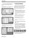
gram of the PLL circuit is shown in Figure 5-3.
The signal from VCO (Voltage-Controlled Oscil-
lator) Q7/Q8 is buffered by Q6 and Q5 and then
applied to pin 2 of IC2. The prescaler in IC2 divides
the VCO signal down so that it is within the frequency
range of the programmable counter.
A reference frequency generated by reference
oscillator and controlled by crystal X1 is applied to pin
15 of IC1. This signal is divided down by a program-
mable divider and provides the reference input to the
phase detector. When the VCO is oscillating at the
correct frequency, the VCO-derived input to the phase
detector is the same frequency as the reference input.


