SWRA004A
20 TRF1500 Integrated Dual-Band RF Receiver User’s Guide
Low-Band LNA Input
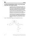
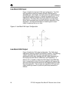
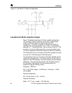
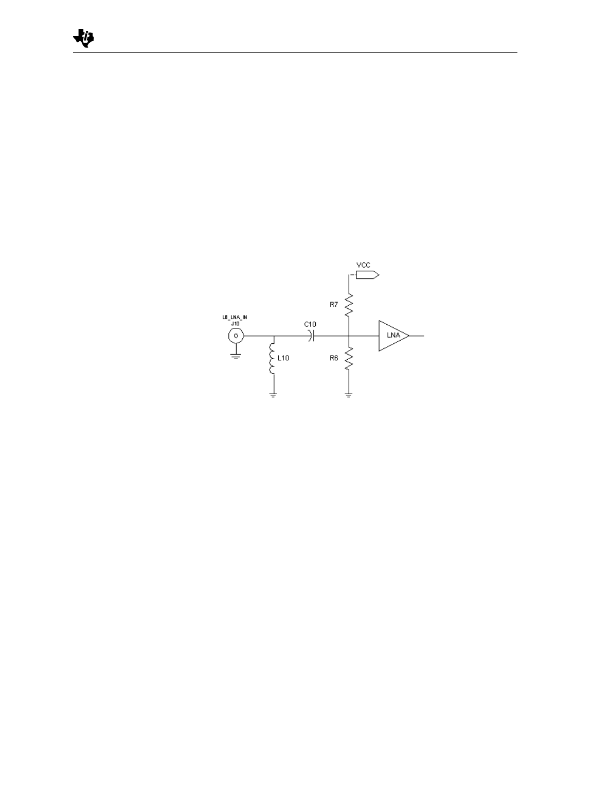
Figure 4 details the low-band LNA input configuration. The LNA
input impedance matching network primarily determines the
cascaded gain, noise figure, and input return loss performance of
the low-band receiver section. A simple high-pass shunt-L (L10)
impedance matching network is used for optimum noise figure
performance. The trade off for this optimization is a lower input
return loss in the pass-band, but with sufficient attenuation in the
stop-band. C10 has minimal effect on matching and is used
mainly to optimize the turn-on time.
Figure 4. Low-Band LNA Input Configuration
Low-Band LNA Output
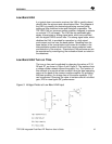
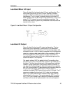
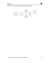
Figure 5 details the LNA output configuration. The LNA output
impedance matching network has several functions. The matching
network optimizes the third order input intercept point (IIP3)
performance while also matching the LNA output impedance to
the Surface Acoustic Wave (SAW) filter input impedance. A
shunt-C (C11) is used to match the LNA output to the SAW filter
input. Increasing the value of the shunt capacitor will improve the
gain and noise figure performance but will degrade the third order
input intercept point. The end user can adjust the LNA input and
output matching network to optimize a particular parameter of
interest.


