


General High-Speed Amplifier Design Considerations
1-8
General Information
1.6 General High-Speed Amplifier Design Considerations
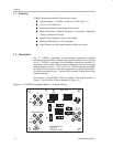
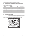
The THS3001 EVM layout has been designed and optimized for use with
high-speed signals and can be used as an example when designing THS3001
applications. Careful attention has been given to component selection,
grounding, power supply bypassing, and signal path layout. Disregard of these
basic design considerations could result in less than optimum performance of
the THS3001 high-speed, current-feedback video operational amplifier.
Surface-mount components were selected because of the extremely low lead
inductance associated with this technology. Also, because surface-mount
components are physically small, the layout can be very compact. This helps
minimize both stray inductance and capacitance.
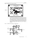
Tantalum power supply bypass capacitors (C1 and C3 for original and C1 and
C2 for Rev. A) at the power input pads help supply currents for rapid, large
signal changes at the amplifier output. The 0.1 µF power supply bypass
capacitors (C2 and C4 for original version and C3 and C4 for Rev. A) were
placed as close as possible to the IC power input pins in order to keep the PCB
trace inductance to a minimum. This improves high-frequency bypassing and
reduces harmonic distortion.
A proper ground plane on both sides of the PCB should always be used with
high-speed circuit design. This provides low-inductive ground connections for
return current paths. In the area of the amplifier IC input pins, however, the
ground plane was removed to minimize stray capacitance and reduce ground
plane noise coupling into these pins. This is especially important for the
inverting pin while the amplifier is operating in the noninverting mode. Because
the voltage at this pin swings directly with the noninverting input voltage, any
stray capacitance would allow currents to flow into the ground plane, causing
possible gain error and/or oscillation. Capacitance variations at the amplifier
IC inverting input pin of less than 1 pF can significantly affect the response of
the amplifier.
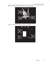
In general, it is always best to keep signal lines as short and as straight as
possible. Sharp 90 corners should be avoided — round corners or a series
of 45 bends should be used, instead. Stripline techniques should also be
incorporated when signal lines are greater than three inches in length. These
traces should be designed with a characteristic impedance of either 50 Ω or
75 Ω, as required by the application. Such signal lines should also be properly
terminated with an appropriate resistor.
Finally, proper termination of all inputs and outputs should be incorporated into
the layout. Unterminated lines, such as coaxial cable, can appear to be a
reactive load to the amplifier IC. By terminating a transmission line with its
characteristic impedance, the amplifier’s load then appears to be purely
resistive and reflections are absorbed at each end of the line. Another
advantage of using an output termination resistor is that capacitive loads are
isolated from the amplifier output. This isolation helps minimize the reduction
in amplifier phase-margin and improves the amplifier stability for improved
performance such as reduced peaking and settling times.