


10
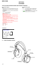
MDR-IF4000
SECTION 3
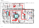
DIAGRAMS
For schematic diagrams.
Note:
• All capacitors are in µF unless otherwise noted. (p: pF)
50 WV or less are not indicated except for electrolytics
and tantalums.
• All resistors are in Ω and
1
/
4
W or less unless otherwise
specified.
• f : internal component.
• C : panel designation.
• A : B+ Line.
• H : adjustment for repair.
• Power voltage is dc 2.4 V and fed with regulated dc power
supply from battery terminal.
•Voltages and waveforms are dc with respect to ground
under no-signal (detuned) conditions.
•Voltages are taken with a VOM (Input impedance 10 MΩ).
Voltage variations may be noted due to normal produc-
tion tolerances.
•Waveforms are taken with a oscilloscope.
Voltage variations may be noted due to normal produc-
tion tolerances.
• Circled numbers refer to waveforms.
• Signal path.
F : ANALOG
J : RF
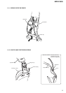
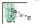
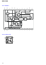
NOTE FOR PRINTED WIRING BOARDS AND SCHEMATIC DIAGRAMS.
For printed wiring boards.
Note:
• X : parts extracted from the component side.
• Y : parts extracted from the conductor side.
• f : internal component.
• : Pattern from the side which enables seeing.
(The other layers' patterns are not indicated.)
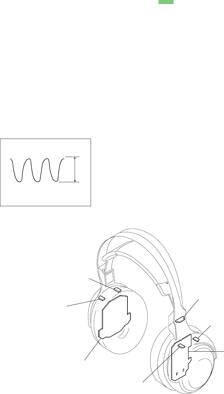
• Waveforms
1V/DIV, 50 ns/DIV
3.5Vp-p
12.288 MHz
1
IC101
rd
OSCO
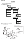
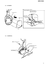
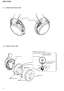
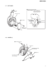
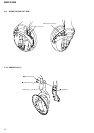
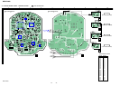
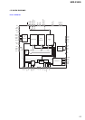
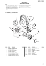
3-1. CIRCUIT BOARDS LOCATION
RX board
BATT boar
d
SW board
RD2 board
(R-CH REAR)
RD1 board
(R-CH FRONT)
RD2 board
(L-CH FRONT)
RD1 board
(L-CH REAR)