


TFA9843AJ_1 © Koninklijke Philips Electronics N.V. 2006. All rights reserved.
Preliminary data sheet Rev. 01 — 28 April 2006 12 of 19
Philips Semiconductors
TFA9843AJ
20 W stereo power amplifier with volume control
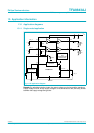
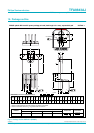
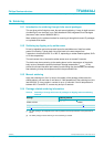
13.2 Printed-circuit board
13.2.1 Layout and grounding
To obtain a high-level system performance, certain grounding techniques are essential.
The input reference grounds have to be tied with their respective source grounds and
must have separate tracks from the power ground tracks; this will prevent the large output
signal currents from interfering with the small AC input signals. The small-signal ground
tracks should be physically located as far as possible from the power ground tracks.
Supply and output tracks should be as wide as possible for delivering maximum output
power.
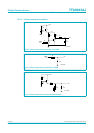
13.2.2 Power supply decoupling
Proper supply bypassing is critical for low-noise performance and high supply voltage
ripple rejection. The respective capacitor location should be as close as possible to the
device and connected to the power ground. Proper power supply decoupling also prevents
unwanted oscillations.
For suppressing higher frequency transients (spikes) on the supply rail a capacitor with
low ESR (typical 100 nF) has to be placed as close as possible to the device. For
suppressing lower frequency noise and ripple signals, a large electrolytic capacitor (e.g.
1000 µF or greater) must be placed close to the device.
The bypass capacitor connected to pin SVR reduces the noise and ripple on the mid rail
voltage. For good THD and noise performance, a low ESR capacitor is recommended.
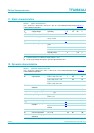
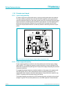
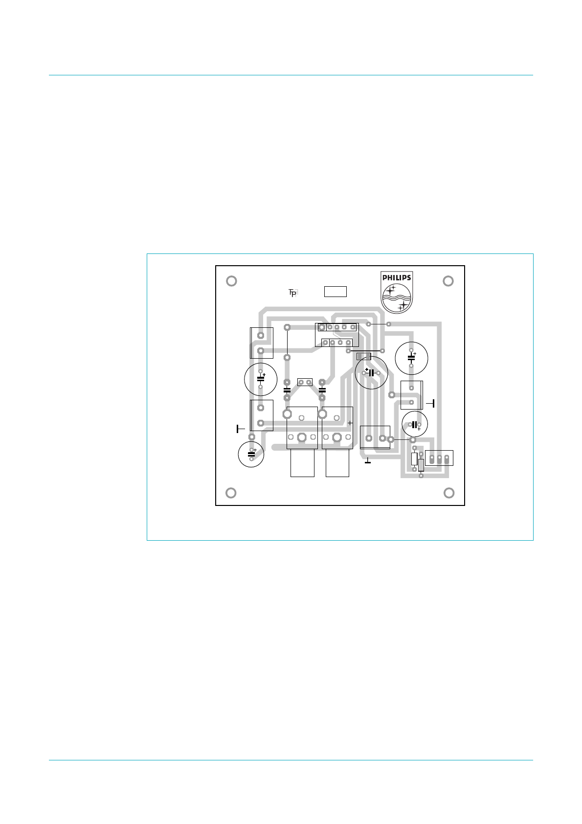
Fig 15. Printed-circuit board layout (single-sided); components view
AUDIO POWER CS NIJMEGEN
27 Jan. 2003 / FP
IN2+ IN1+
MUTE
SB ON
TVA
TFA9843J
−SE2+
−SE1+
+V
P
1000 µF
1000 µF
1000 µF
BTL1/2
1
22
µF
10 kΩ
10
kΩ
mce506
100 nF
150 µF
220
nF
220
nF
MODE
SGND
SVR
SVR
CIV
CIV