


2001 Jul 23 12
Philips Semiconductors Preliminary specification
Power amplifier with load detection and
auto BTL/SE selection
TDA8586
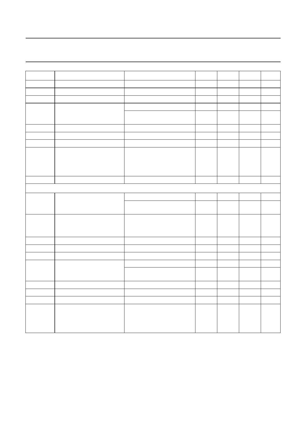
Notes
1. Tolerances on the mute level is tight because of the usage of this pin for integration during load detection.
2. The output power is measured directly on the pins of the IC.
3. The noise output is measured in a bandwidth of 20 Hz to 20 kHz.
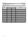
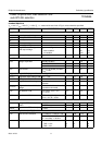
G
v
voltage gain V
i(rms)
=15mV 313233dB
∆G
v
channel unbalance V
i(rms)
=15mV −0.7 0 +0.7 dB
α
cs
channel separation P
o
= 2 W; f
i
= 1 kHz; R
L
=4Ω 45 55 − dB
V
OO
DC output offset voltage V
P
= 14.4 V; on condition − 0 100 mV
V
P
= 14.4 V; R
L
=4Ω;
mute condition
− 10 20 mV
V
n(o)
noise output voltage on R
s
=1kΩ; V
P
= 14.4 V; note 3 − 100 150 µV
V
n(o)(mute)
noise output voltage mute note 3 − 020µV
V
o(mute)
output voltage mute V
i(rms)
=1V − 3 500 µV
SVRR supply voltage ripple rejection: R
s
=0Ω; f
i
= 1 kHz;
V
ripple
= 2 V (p-p)
on condition 45 55 − dB
mute condition 55 70 − dB
Z
i
input impedance input referenced to ground 40 60 90 kΩ
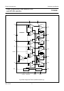
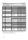
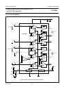
Quad SE application (see Fig.8)
THD total harmonic distortion f
i
= 1 kHz; P
o
= 1 W; R
L
=4Ω− 0.05 0.15 %
45 Hz < f
i
< 10 kHz; P
o
=1W;
R
L
=4Ω; filter: f < 30 kHz
− 0.5 − %
P
o
output power V
P
= 14.4 V; R
L
=4Ω; note 2
THD = 0.5% 4 4.5 − W
THD = 10% 5 6 − W
G
v
voltage gain V
i(rms)
=15mV 252627dB
∆G
v
channel unbalance V
i(rms)
=15mV −0.7 0 +0.7 dB
α
cs
channel separation P
o
= 2 W; f
i
= 1 kHz; R
L
=4Ω 40 50 − dB
V
OO
DC output offset voltage V
P
= 14.4 V; on condition − 0 100 mV
V
P
= 14.4 V; R
L
=4Ω;
mute condition
− 10 20 mV
V
n(o)
noise output voltage on R
s
=1kΩ; V
P
= 14.4 V; note 3 − 80 150 µV
V
n(o)(mute)
noise output voltage mute note 3 − 020µV
V
o(mute)
output voltage mute V
i(rms)
=1V − 3 500 µV
SVRR supply voltage ripple rejection R
s
=0Ω; f
i
= 1 kHz;
V
ripple
= 2 V (p-p)
on condition 43 47 − dB
mute condition 55 70 − dB
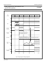
SYMBOL PARAMETER CONDITIONS MIN. TYP. MAX. UNIT