


2001 Jul 23 11
Philips Semiconductors Preliminary specification
Power amplifier with load detection and
auto BTL/SE selection
TDA8586
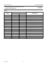
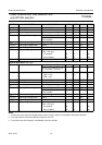
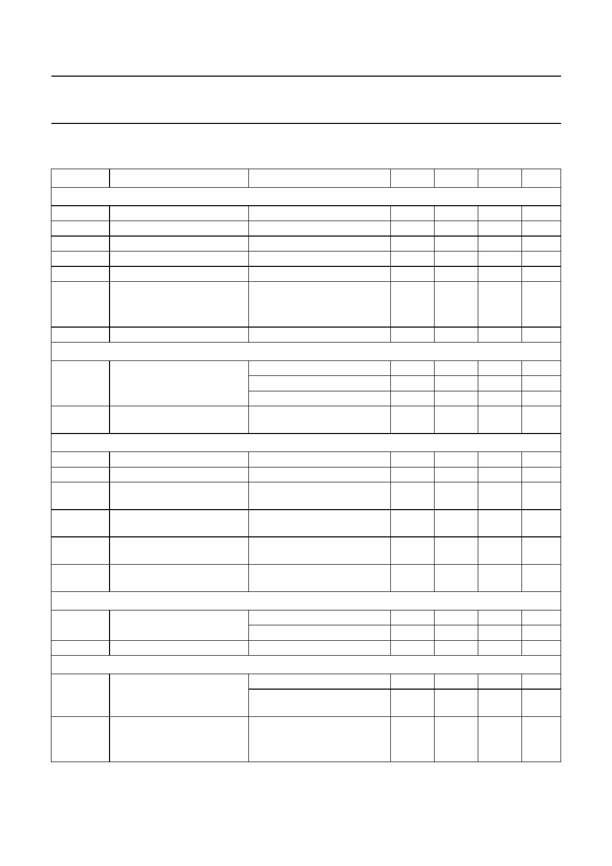
CHARACTERISTICS
V
P
= 14.4 V; T
amb
=25°C; f
i
= 1 kHz; R
L
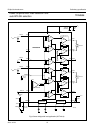
= ∞; measured in test circuit of Fig.8; unless otherwise specified.
SYMBOL PARAMETER CONDITIONS MIN. TYP. MAX. UNIT
Supplies
V
P
operating supply voltage 8.0 14.4 18 V
I
q(tot)
total quiescent current SE mode − 140 170 mA
I
stb
standby current − 1 100 µA
V
O
DC output voltage V
P
= 14.4 V − 7.0 − V
V
P(mute)
low supply voltage mute 6.0 7.0 8.0 V
V
o
single-ended and bridge-tied
load output voltage
V
P
= 14.4 V; R
L
=4Ω
mute condition −−20 mV
on condition −−100 mV
V
I
DC input voltage V
P
= 14.4 V − 4.0 − V
PIN MSO
V
MSO
voltage at pin MSO standby condition 0 − 0.8 V
mute condition; note 1 2.0 3.0 4 V
on condition 8.0 − 10.5 V
I
MSO
input current mute pin at standby condition;
V
MSO
< 0.8 V
− 540µA
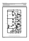
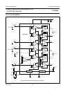
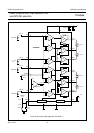
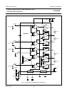
Diagnostic; output buffer (open-collector); see Figs 7 to 8
V
DIAG(L)
diagnostic output voltage LOW I
sink
=1mA − 0.3 0.8 V
I
LI
leakage current V
DIAG
= 14.4 V −−1µA
V
DIAG(or)
diagnostic override voltage in mute mode after load
detection
10.5 − 18 V
V
DIAG(4ch)
diagnostic 4 channel indication
voltage
mute, after load detection with
4 speakers connected
− 0.3 0.8 V
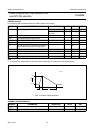
CD2 clip detector LOW THD mode; V
DIAG
>3V;
R=10kΩ
0.5 2 3.5 %
CD10 clip detector HIGH THD mode (default);
V
DIAG
>3V; R=10kΩ
71013%
CLIP DETECT CONTROL PIN
V
DDDSEL
voltage at DDD select pin to
obtain:
10% DDD 0 − 1V
2% DDD 3 − 6V
I
DDDSEL
Input current DDD select pin V
DDDSEL
=5V 15 − 140 µA
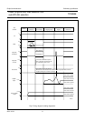
Stereo BTL application (see Fig.7)
THD total harmonic distortion f
i
= 1 kHz; P
o
= 1 W; R
L
=4Ω− 0.05 0.15 %
45 Hz < f
i
< 10 kHz; P
o
=1W;
R
L
=4Ω; filter: f < 30 kHz
− 0.3 − %
P
o
output power V
P
= 14.4 V; R
L
=4Ω; note 2
THD = 0.5% 14 15 − W
THD = 10% 17 21 − W