


2002 Oct 18 7
Philips Semiconductors Product specification
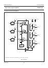
Triple video output amplifier TDA6107JF
Notes
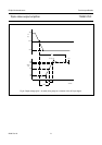
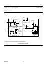
1. See also Fig.5 for the typical DC-to-DC transfer of V
I
to V
O(oc)
.
2. The ratio of the change in supply voltage to the change in input voltage when there is no change in output voltage.
∆t
Pco
difference in cathode output
propagation time 50% input to
50% output (pins 7 and 8,
7 and 9 and 8 and 9)
V
o(c)
= 100 V (p-p) square
wave; f < 1 MHz;
t
r
=t
f
=40ns
(pins 1, 2 and 3)
−10 0 +10 ns
t
o(r)
cathode output rise time
10% output to 90% output
(pins 7, 8 and 9)
V
o(c)
= 50 to 150 V square
wave; f < 1 MHz; t
f
=40ns
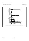
(pins 1, 2 and 3); see Fig.6
67 91 113 ns
t
o(f)
cathode output fall time
90% output to 10% output
(pins 7, 8 and 9)
V
o(c)
= 150 to 50 V square
wave; f < 1 MHz; t
r
=40ns
(pins 1, 2 and 3); see Fig.7
67 91 113 ns
t
st
settling time 50% input to
99% < output < 101%
(pins 7, 8 and 9)
V
o(c)
= 100 V (p-p) square
wave; f < 1 MHz;
t
r
=t
f
=40ns
(pins 1, 2 and 3);
see Figs 6 and 7
−−350 ns
SR slew rate between
50Vto(V
DD
− 50 V)
(pins 7, 8 and 9)
V
i
= 4 V (p-p) square wave;
f < 1 MHz; t
r
=t
f
=40ns
(pins 1, 2 and 3)
− 900 − V/µs
O
v
cathode output voltage
overshoot (pins 7, 8 and 9)
V
o(c)
= 100 V (p-p) square
wave; f < 1 MHz;
t
r
=t
f
=40ns
(pins 1, 2 and 3);
see Figs 6 and 7
− 2 − %
PSRR power supply rejection ratio f < 50 kHz; note 2 − 55 − dB
α
ct(DC)
DC crosstalk between
channels
−−50 − dB
SYMBOL PARAMETER CONDITIONS MIN. TYP. MAX. UNIT