


2002 Oct 18 11
Philips Semiconductors Product specification
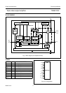
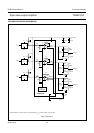
Triple video output amplifier TDA6107JF
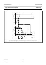
Cathode output
The cathode output is protected against peak current
(caused by positive voltage peaks during high-resistance
flash) of 3 A maximum with a charge content of 100 µC
(1)
.
The cathode is also protected against peak currents
(caused by positive voltage peaks during low-resistance
flash) of 6 A maximum with a charge content of 100 nC
(1)
.
The DC voltage of V
DD
(pin 6) must be within the operating
range of 180 to 210 V during the peak currents.
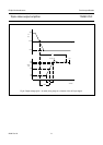
Flashover protection
The TDA6107JF incorporates protection diodes against
CRT flashover discharges that clamp the cathodes output
voltage up to a maximum of V
DD
+V
diode
.
To limit the diode current an external 1.5 kΩ carbon
high-voltage resistor in series with the cathode output and
a 2 kV spark gap are needed (for this resistor value, the
CRT has to be connected to the main PCB
(1)
.
V
DD
must be decoupled to GND:
1. With a capacitor >20 nF with good HF behaviour
(e.g. foil); this capacitor must be placed as close as
possible to pins 6 and 4, but definitely within 5 mm.
2. With a capacitor >3.3 µF on the picture tube base
print, depending on the CRT size.
Switch-off behaviour
The switch-offbehaviour ofthe TDA6107JFis controllable.
This is because the output pins of the TDA6107JF are still
under control of the input pins for low power supply
voltages (approximately 30 V and higher).
Bandwidth
The addition of the flash resistor produces a decreased
bandwidth and increases the rise and fall times; see
“Application Note AN96072”
.
Dissipation
Regarding dissipation, distinction must first be made
between static dissipation (independent of frequency) and
dynamic dissipation (proportional to frequency).
The static dissipation of the TDA6107JF is due to voltage
supply currents and load currents in the feedback network
and CRT.
The static dissipation P
stat
equals:
Where:
V
DD
= supply voltage
I
DD
= supply current
V
OC
= DC value of cathode voltage
I
OC
= DC value of cathode current.
The dynamic dissipation P
dyn
equals:
Where:
C
L
= load capacitance
C
int
= internal load capacitance (≈4 pF)
f
i
= input frequency
V
oc(p-p)
= output voltage (peak-to-peak value)
δ = non-blanking duty cycle.
The IC must be mounted on the picture tube base print to
minimize the load capacitance C
L
.
(1)External protection against higher currents is described
in
“Application Note AN96072”
.
P
stat
V
DD
I
DD
3V
OC
I
OC
××+×=
P
dyn
3V
DD
C
L
C
int
+()f
i
V
oc(p-p)
δ×××××=