


2002 Oct 18 3
Philips Semiconductors Product specification
Triple video output amplifier TDA6107JF
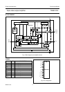
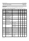
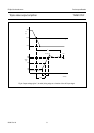
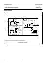
BLOCK DIAGRAM
handbook, full pagewidth
MBL525
TDA6107JF
V
DD
6
1, 2, 3
4
9, 8, 7
V
oc(3),
V
oc(2),
V
oc(1)
5
I
o(m)
R
f
MIRROR 5
DIFFERENTIAL
STAGE
VIP
REFERENCE
CURRENT
SOURCE
R
i
V
i(1)
,
V
i(2)
,
V
i(3)
R
a
3×
3×
CASCODE 1
CASCODE 2
MIRROR 2
1×
MIRROR 4
MIRROR 3
MIRROR 1
THERMAL
PROTECTION
CIRCUIT
1×
Fig.1 Block diagram (one amplifier shown).
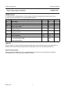
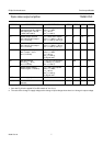
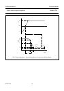
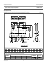
PINNING
SYMBOL PIN DESCRIPTION
V
i(1)
1 inverting input 1
V
i(2)
2 inverting input 2
V
i(3)
3 inverting input 3
GND 4 ground (fin)
I
om
5 black-current measurement output
V
DD
6 supply voltage
V
oc(3)
7 cathode output 3
V
oc(2)
8 cathode output 2
V
oc(1)
9 cathode output 1
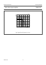
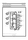
handbook, halfpage
V
i(1)
V
i(2)
V
i(3)
GND
I
om
V
DD
V
oc(3)
V
oc(2)
V
oc(1)
1
2
3
4
5
6
7
8
9
TDA6107JF
MBL524
Fig.2 Pin configuration.