


March 1994 5
Philips Semiconductors Preliminary specification
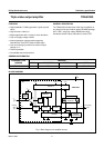
Triple video output amplifier TDA6103Q
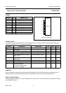
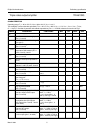
CHARACTERISTICS
Operating range: T
j
= −20 to 150 °C; V
DD
= 180 to 210 V; V
ip
= 1 to 4 V.
Test conditions (unless otherwise specified): T
amb
= 25 °C; V
DD
= 200 V; V
ip
= 1.3 V; V
oc1
= V
oc2
= V
oc3
=
1
⁄
2
V
DD
;
C
L
= 10 pF (C
L
consists of parasitic and cathode capacitance); R
th h-a
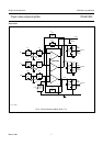
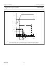
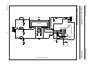
= 18 K/W; measured in test circuit Fig.5.
SYMBOL PARAMETER CONDITIONS MIN. TYP. MAX. UNIT
I
DD
quiescent supply current 7.0 9.25 11.5 mA
I
bias
input bias current inverting inputs
(pins 1, 2 and 3)
−5 −1+1µA
I
bias
input bias current non-inverting
input (pin 5)
−15 −3+1µA
V
i(offset)
input offset voltage
(pins 1, 2 and 3)
−50 − +50 mV
∆V
i(offset)
differential input offset voltage
temperature drift between pins 1
and 5; 2 and 5; 3 and 5
− tbf − mV/K
C
icm
common-mode input capacitance
(pins 1, 2 and 3)
− 5 − pF
C
icm
common-mode input capacitance
(pin 5)
− 10 − pF
C
idm
differential mode input capacitance
between 1 and 5; 2 and 5; 3 and 5
− 1 − pF
V
oc(min)
minimum output voltage
(pins 7, 8 and 9)
V
1−5
= V
2−5
= V
3−5
= −1V − 510V
V
oc(max)
maximum output voltage
(pins 7, 8 and 9)
V
1−5
= V
2−5
= V
3−5
= 1 V;
note 1
V
DD
− 10 V
DD
− 6 − V
GB gain-bandwidth product of
open-loop gain:
V
oc1, 2, 3
/V
i1-5, 2-5, 3-5
f = 500 kHz − 0.75 − GHz
B
S
small signal bandwidth
(pins 7, 8 and 9)
V
oc(p-p)
= 60 V 6 7.5 − MHz
B
L
large signal bandwidth
(pins 7, 8 and 9)
V
oc(p-p)
= 100 V 5 7 − MHz
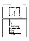
t
pd
cathode output propagation delay
time 50% input to 50% output
(pins 7, 8 and 9)
V
oc(p-p)
= 100 V square
wave; f < 1 MHz;
t
r
=t
f
= 40 ns (pins 1, 2
and 3); see Figs 7 and 8
− 38 − ns
∆t
p
difference in cathode output
propagation time 50% input to
50% output (pins 7 and 8, 7 and 9
and 8 and 9)
V
oc(p-p)
= 100 V square
wave; f < 1 MHz;
t
r
=t
f
= 40 ns (pins 1, 2
and 3)
−10 0 +10 ns
t
r
cathode output rise time 10%
output to 90% output
(pins 7, 8 and 9)
V
oc
= 50 to 150 V square
wave; f < 1 MHz; t
f
= 40 ns
(pins 1, 2 and 3); see Fig.7
48 60 73 ns
t
f
cathode output fall time 90% output
to 10% output (pins 7, 8 and 9)
V
o
= 150 to 50 V square
wave; f < 1 MHz; t
r
= 40 ns
(pins 1, 2 and 3); see Fig.8
48 60 73 ns