


March 1994 3
Philips Semiconductors Preliminary specification
Triple video output amplifier TDA6103Q
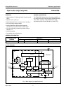
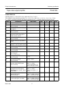
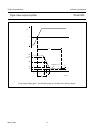
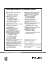
PINNING
SYMBOL PIN DESCRIPTION
V
i1
1 inverting input 1
V
i2
2 inverting input 2
V
i3
3 inverting input 3
GND 4 ground, fin
V
ip
5 non-inverting input
V
DD
6 supply voltage
V
oc3
7 cathode output 3
V
oc2
8 cathode output 2
V
oc1
9 cathode output 1
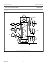
Fig.2 Pin configuration.
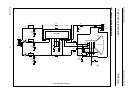
1
2
3
4
5
6
7
8
9
MGA969
V
i1
GND
V
DD
V
oc3
TDA6103Q
V
i2
V
i3
V
oc2
V
oc1
V
ip
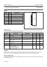
LIMITING VALUES
In accordance with the Absolute Maximum Rating System (IEC 134). Voltages measured with respect to GND (pin 4);
currents as specified in Fig.1; unless otherwise specified.
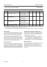
HANDLING
Inputs and outputs are protected against electrostatic discharge in normal handling. However, to be totally safe, it is
desirable to take normal precautions appropriate to handling MOS devices (see
“Handling MOS Devices”
).
QUALITY SPECIFICATION
Quality specification
“SNW-FQ-611 part E”
is applicable and can be found in the
“Quality reference pocketbook”
(ordering
number 9398 510 34011).
SYMBOL PARAMETER CONDITIONS MIN. MAX. UNIT
V
DD
supply voltage 0 250 V
V
i
input voltage 0 12 V
V
idm
differential mode input voltage −6+6V
V
oc
cathode output voltage 0 V
DD
V
I
ocsmL
LOW non-repetitive peak cathode
output current
flashover discharge = 50 µC05A
I
ocsmH
HIGH non-repetitive peak cathode
output current
flashover discharge = 100 nC 0 10 A
T
stg
storage temperature −55 +150 °C
T
j
junction temperature −20 +150 °C
V
es
electrostatic handling
human body model (HBM) − tbf V
machine model (MM) − tbf V