


April 1985 5
Philips Semiconductors Product specification
I.F. amplifier and demodulator for
multistandard TV receivers
TDA2549
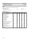
Notes to the characteristics
1.
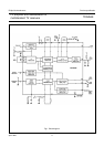
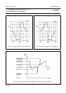
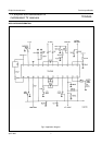
2. Measured in application of Fig. 5.
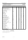
A.F.C. output voltage swing V
15-3
10 −−V
Change of frequency required for a.f.c.
output voltage swing of 10 V ∆f − 70 200 kHz
A.F.C. switch off for a voltage lower than: V
17-3
−−1,5 V
A.F.C. inverter switch
positive a.f.c. (Fig.2) V
16-3
0 − 1,5 V
negative a.f.c. (Fig.3) V
16-3
4 − 12 V
Tuner A.G.C.
Leakage current I
10
−−15 µA
Saturation voltage
I
10
= 0,3 mA V
10-3
− 0,1 0,3 V
take-over point LOW V
i
−−3mV
take-over point HIGH V
i
10 −−mV
Signal expansion at G
v
= 50 dB ∆V
22-3
−−0,5 dB
Negative modulation (Fig.4)
white spot inverter threshold level V
22-3
− 4,6 − V
white spot insertion level V
22-3
− 3,2 − V
noise inverter threshold level V
22-3
− 0,9 − V
noise insertion level V
22-3
− 2,5 − V
Positive modulation a.g.c. detector
reference level V
11-3
3,0 3,2 3,4 V
Auxiliary video input signal for V
o(p-p)
=2 V V
12-3
0,7 1 1,4 V
Auxiliary video output
output signal (note 2) V
14-3
− 1 − V
top sync level V
14-3
123V
output impedance |Z
14-3
| − 7 −Ω
Levels for video switches
positive video V
2-3
−−1V
negative video V
2-3
3 −−V
internally demodulated signal V
23-3
−−1V
auxiliary video signal V
23-3
3 −−V
PARAMETER SYMBOL MIN. TYP. MAX. UNIT
Signal to– noise ratio S/N–
V
o
black-to-white
V
n rms()
at B 5 MHz=
-----------------------------------------------------------
=