


Philips Semiconductors Product specification
SA5223Wide dynamic range AGC transimpedance amplifier(150MHz)
1995 Oct 24
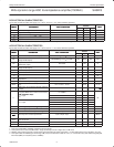
5
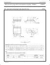
1
2
3
4
8
7
6
5
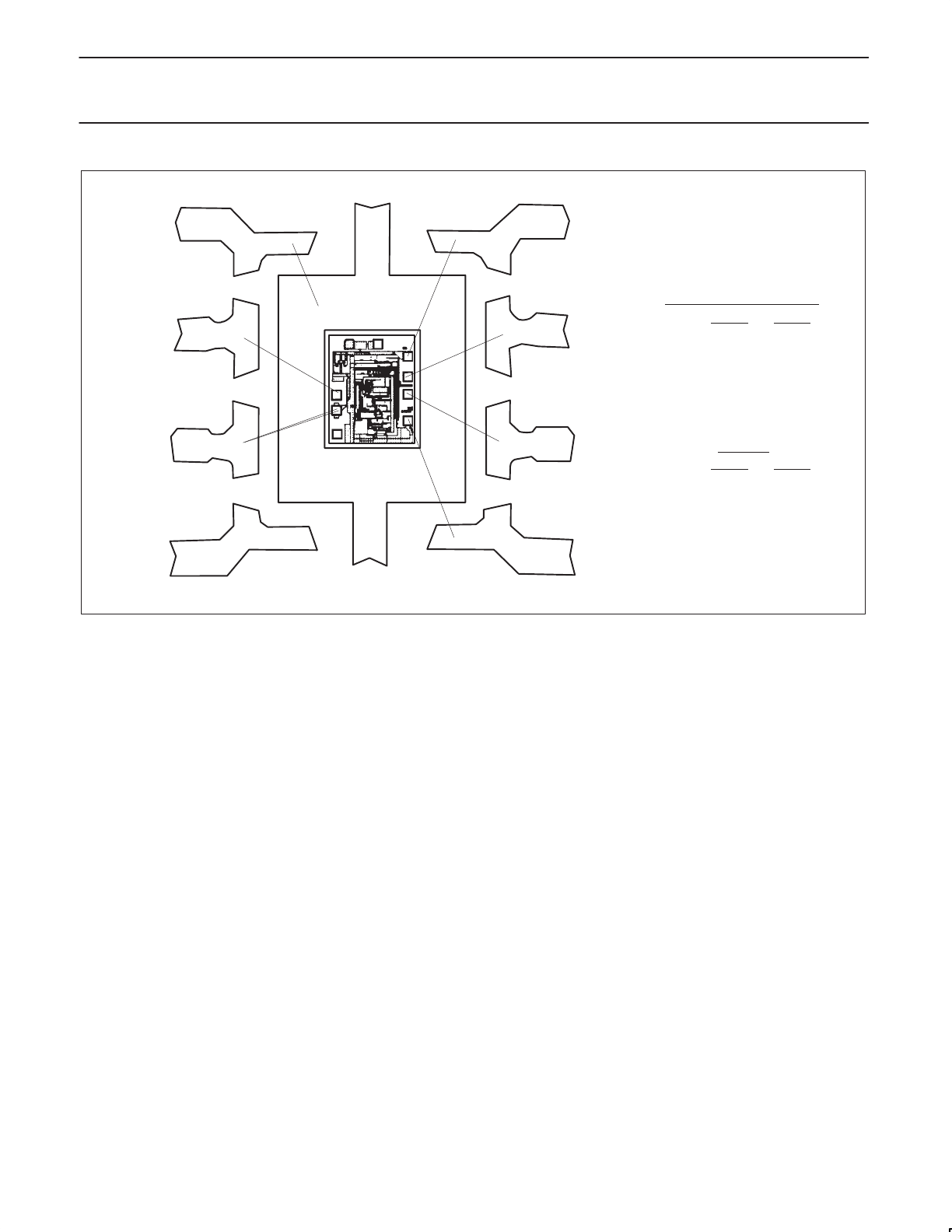
SD00507
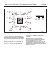
GND
G1
IN
V
CC
OUT
OUTB
G2
GND
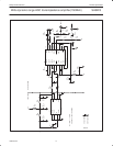
PAD CENTER LOCATIONS
X(mm) Y(mm)
GND1 -0.400 -0.053
IN -0.400 -0.223
GND2 +0.400 -0.342
OUT +0.400 -0.046
OUTB +0.400 +0.154
V
CC
+0.400 +0.380
DIE SIZE
X(mm) Y(mm)
1.08 1.32
NC NC
NC
Figure 1. SA5223 Bonding Diagram
Die Sales Disclaimer
Due to the limitations in testing high frequency and other parameters
at the die level, and the fact that die electrical characteristics may
shift after packaging, die electrical parameters are not specified and
die are not guaranteed to meet electrical characteristics (including
temperature range) as noted in this data sheet which is intended
only to specify electrical characteristics for a packaged device.
All die are 100% functional with various parametrics tested at the
wafer level, at room temperature only (25°C), and are guaranteed to
be 100% functional as a result of electrical testing to the point of
wafer sawing only. Although the most modern processes are
utilized for wafer sawing and die pick and place into waffle pack
carriers, it is impossible to guarantee 100% functionality through this
process. There is no post waffle pack testing performed on
individual die.
Since Philips Semiconductors has no control of third party
procedures in the handling or packaging of die, Philips
Semiconductors assumes no liability for device functionality or
performance of the die or systems on any die sales.
Although Philips Semiconductors typically realizes a yield of 85%
after assembling die into their respective packages, with care
customers should achieve a similar yield. However, for the reasons
stated above, Philips Semiconductors cannot guarantee this or any
other yield on any die sales.