


Philips Semiconductors Product specification
SA5223Wide dynamic range AGC transimpedance amplifier(150MHz)
1995 Oct 24
3
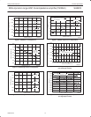
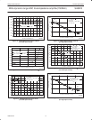
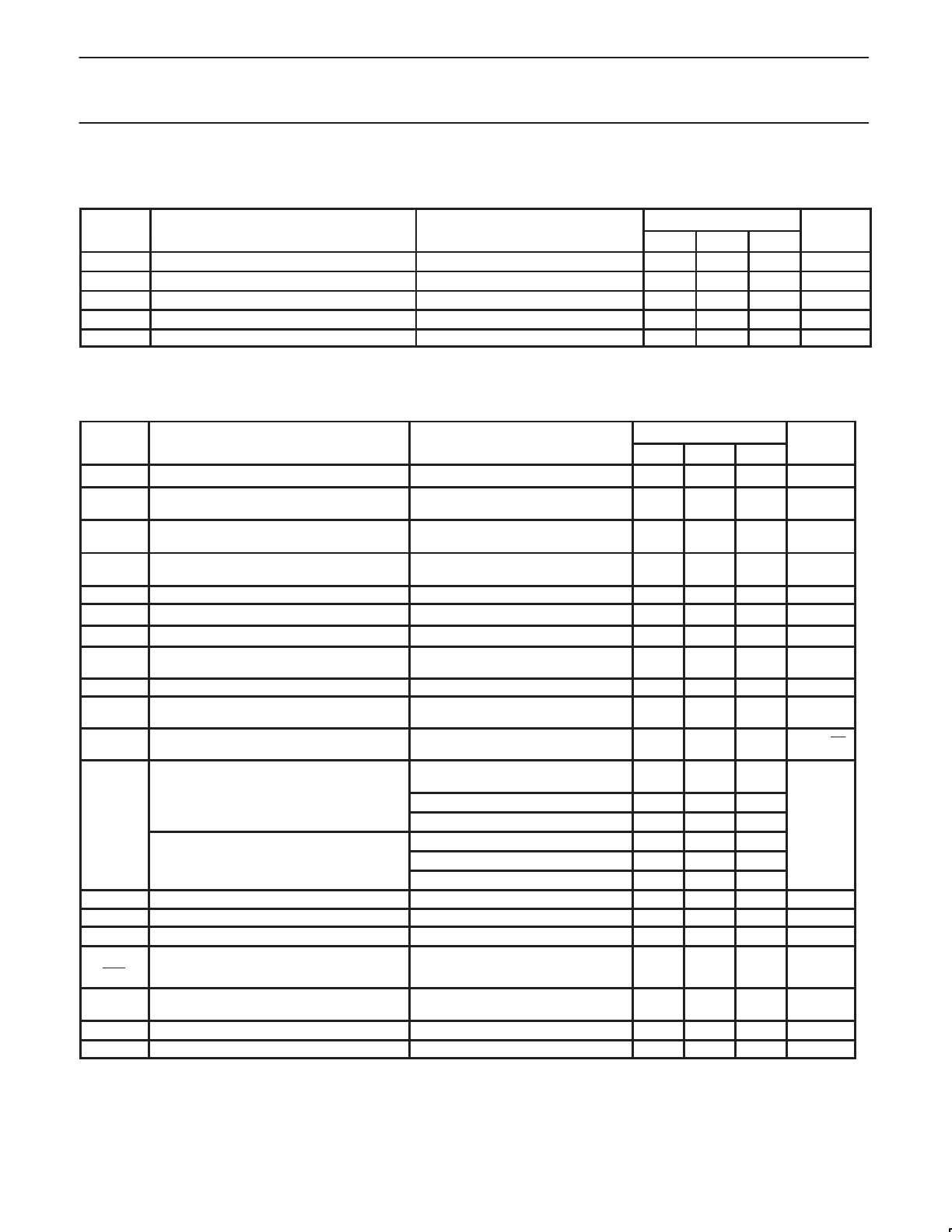
DC ELECTRICAL CHARACTERISTICS
Typical data and Min and Max limits apply at T
A
= 25°C, and V
CC
= +5V, unless otherwise specified.
SYMBOL
PARAMETER
TEST CONDITIONS
SA5223
UNIT
SYMBOL
PARAMETER
TEST
CONDITIONS
Min Typ Max
UNIT
V
IN
Input bias voltage 1.3 1.55 1.8 V
V
O
±
Output bias voltage 2.9 3.2 3.5 V
V
OS
Output offset voltage (V
PIN6
- V
PIN7
) -200 80 +200 mV
I
CC
Supply current 15 22 29 mA
I
OMAX
Output sink/source current 1.5 2 mA
NOTE: Standard deviations are estimated from design simulations to represent manufacturing variations over the life of the product.
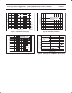
AC ELECTRICAL CHARACTERISTICS
Typical data and Min and Max limits apply at T
A
= 25°C and V
CC
= +5V, unless otherwise specified.
SYMBOL
PARAMETER
TEST CONDITIONS
SA5223
UNIT
SYMBOL
PARAMETER
TEST
CONDITIONS
Min Typ Max
UNIT
R
T
Transresistance (differential output)
DC tested, R
L
= ∞, I
IN
= 0-1µA
90 125 160 kΩ
R
T
Transresistance
(single-ended output)
DC tested, R
L
= ∞, I
IN
= 0-1µA
45 62.5 80 kΩ
R
O
Output resistance
(differential output)
DC tested 140 Ω
R
O
Output resistance
(single-ended output)
DC tested 70 Ω
f
3dB
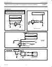
Bandwidth (-3dB) Test Circuit 1 110 150 MHz
R
IN
Input resistance DC tested 250
Ω
C
IN
Input capacitance
1
0.7
pF
C
INT
Input capacitance including Miller multiplied
capacitance
4.0
pF
∆R/∆V Transresistance power supply sensitivity V
CC1
= V
CC2
= 5 ±0.5V 3 %/V
∆R/∆T
Transresistance ambient temperature sensi-
tivity
∆T
A
= T
A
MAX
- T
A
MIN
0.09
%/
o
C
I
IN
RMS noise current spectral density (referred
to input)
2
Test Circuit 2, f = 10MHz 1.17
pAń Hz
Ǹ
Integrated RMS noise current over the band-
idth (referred to inp t)
Test circuit 2,
∆f = 50MHz
7
w
idth
(
re
f
erre
d
t
o
i
npu
t)
C
S
=
0.1
p
F
∆f = 100MHz 12
I
T
C
S
=
0
.
1F
∆f = 150MHz 16
nA
T
∆f = 50MHz 8
C
S
= 0.4pF ∆f = 100MHz 13
∆f = 150MHz 18
PSRR Power supply rejection ratio (change in V
OS
) DC Tested, ∆V
CC
= ±0.5V –55 dB
PSRR Power supply rejection ratio
3
f = 1.0MHz, Test Circuit 3 –20 dB
V
OLMAX
Maximum differential output AC voltage I
i
= 0–2mA peak AC 800 mV
dR
T
dt
AGC loop time constant parameter
4
10µA to 20µA steps 1 dB/ms
I
INMAX
Maximum input amplitude for output duty
cycle of 50 ±5%
Test circuit 4 +2 mA
t
r
, t
f
Output rise and fall times 10 – 90% 2.2 ns
t
D
Group delay f = 10MHz 2.2 ns
NOTES:
1. Does not include Miller-multiplied capacitance of input device.
2. Noise performance measured differential. Single-ended output noise is higher due to CM noise.
3. PSRR is output referenced and is circuit board layout dependent at higher frequencies. For best performance use a RF filter in V
CC
line.
4. This implies that the SA5223 gain will change 1dB (10%) in the absence of data for 1ms (i.e., can handle bursty data without degrading Bit
Error Rate (BER) for 100,000 cycles at 100MHz).