


Philips Semiconductors Product specification
SA5205AWide-band high-frequency amplifier
1997 Nov 07
8
POWER DISSIPATION CONSIDERATIONS
When using the part at elevated temperature, the engineer should con-
sider the power dissipation capabilities.
At the nominal supply voltage of 6V, the typical supply current is
25mA (32mA Max). For operation at supply voltages other than 6V,
see Figure 3 for I
CC
versus V
CC
curves. The supply current is
inversely proportional to temperature and varies no more than 1mA
between 25°C and either temperature extreme. The change is 0.1%
per over the range.
The recommended operating temperature ranges are air-mount
specifications. Better heat sinking benefits can be realized by
mounting the D package body against the PC board plane.
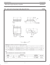
PC BOARD MOUNTING
In order to realize satisfactory mounting of the SA5205A to a PC
board, certain techniques need to be utilized. The board must be
double-sided with copper and all pins must be soldered to their
respective areas (i.e., all GND and V
CC
pins on the SO package).
The power supply should be decoupled with a capacitor as close to
the V
CC
pins as possible and an RF choke should be inserted
between the supply and the device. Caution should be exercised in
the connection of input and output pins. Standard microstrip should
be observed wherever possible. There should be no solder bumps
or burrs or any obstructions in the signal path to cause launching
problems. The path should be as straight as possible and lead
lengths as short as possible from the part to the cable connection.
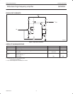
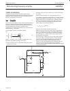
Another important consideration is that the input and output should
be AC coupled. This is because at V
CC
=6V, the input is
approximately at 1V while the output is at 3.1V. The output must be
decoupled into a low impedance system or the DC bias on the
output of the amplifier will be loaded down causing loss of output
power. The easiest way to decouple the entire amplifier is by
soldering a high frequency chip capacitor directly to the input and
output pins of the device. This circuit is shown in Figure 18. Follow
these recommendations to get the best frequency response and
noise immunity. The board design is as important as the integrated
circuit design itself.
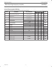
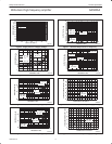
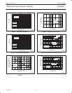
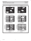
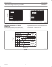
SCATTERING PARAMETERS
The primary specifications for the SA5205A are listed as
S-parameters. S-parameters are measurements of incident and
reflected currents and voltages between the source, amplifier and
load as well as transmission losses. The parameters for a two-port
network are defined in Figure 19.
Actual S-parameter measurements using an HP network analyzer
(model 8505A) and an HP S-parameter tester (models 8503A/B) are
shown in Figure 20.
Values for the figures below are measured and specified in the data
sheet to ease adaptation and comparison of the SA5205A to other
high-frequency amplifiers.
5205A
V
OUT
V
IN
V
CC
AC
COUPLING
CAPACITOR
RF CHOKE
DECOUPLING
CAPACITOR
AC
COUPLING
CAPACITOR
SR00232
Figure 18. Circuit Schematic for Coupling and Power Supply
Decoupling
a. Two-Port Network Defined
b.
S
21
S
12
S
22
S
11
POWER AVAILABLE FROM
GENERATOR AT INPUT PORT
POWER REFLECTED
FROM INPUT PORT
S
11
=
POWER REFLECTED
FROM OUTPUT PORT
POWER AVAILABLE FROM
GENERATOR AT OUTPUT PORT
S
22
=
REVERSE TRANSDUCER
POWER GAIN
S
12
=
S
11
— INPUT RETURN LOSS
S
12
— REVERSE TRANSMISSION LOSS
OSOLATION
S
21
— FORWARD TRANSMISSION LOSS
OR INSERTION GAIN
S
21
= TRANSDUCER POWER GAIN
S
22
— OUTPUT RETURN LOSS
SR00233
Figure 19.