


SA58670A_2 © NXP B.V. 2008. All rights reserved.
Product data sheet Rev. 02 — 23 October 2008 5 of 24
NXP Semiconductors
SA58670A
2.1 W/channel stereo class-D audio amplifier
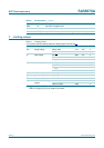
8. Static characteristics
[1] V
DD
is the supply voltage on pins PVDD and pin AVDD.
GND is the ground supply voltage on pins PGND and pin AGND.
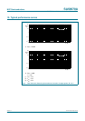
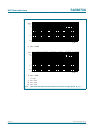
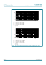
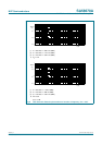
Table 4. Static characteristics
T
amb
=25
°
C; unless otherwise specified
[1]
.
Symbol Parameter Conditions Min Typ Max Unit
V
DD
supply voltage operating 2.5 - 5.5 V
I
DD
supply current V
DD
= 2.5 V; no load - 4 6 mA
V
DD
= 3.6 V; no load - 5 7.5 mA
V
DD
= 5.5 V; no load - 6 9 mA
I
DD(sd)
shutdown mode supply current no input signal;
V
SDR
=V
SDL
= GND
- 10 1000 nA
PSRR power supply rejection ratio V
DD
= 2.5 V to 5.5 V - −75 −55 dB
V
i(cm)
common-mode input voltage 0.5 - V
DD
− 0.8 V
CMRR common mode rejection ratio inputs are shorted together;
V
DD
= 2.5 V to 5.5 V
- −69 −50 dB
V
IH
HIGH-level input voltage V
DD
= 2.5 V to 5.5 V;
pins
SDL, SDR, G0, G1
1.3 - V
DD
V
V
IL
LOW-level input voltage V
DD
= 2.5 V to 5.5 V;
pins
SDL, SDR, G0, G1
0 - 0.35 V
I
IH
HIGH-level input current V
DD
= 5.5 V; V
I
=V
DD
--50 µA
I
IL
LOW-level input current V
DD
= 5.5 V; V
I
=0V --5 µA
f
sw
switching frequency V
DD
= 2.5 V to 5.5 V 250 300 350 kHz
G
v(cl)
closed-loop voltage gain V
G0
= V
G1
= 0.35 V 5.5 6 6.5 dB
V
G0
= V
DD
; V
G1
= 0.35 V 11.5 12 12.5 dB
V
G0
= 0.35 V; V
G1
= V
DD
17.5 18 18.5 dB
V
G0
= V
G1
= V
DD
23.5 24 24.5 dB
Pins OUTLP, OUTLN, OUTRP and OUTRN
R
DSon
drain-source on-state resistance V
DD
= 2.5 V - 700 - mΩ
V
DD
= 3.6 V - 570 - mΩ
V
DD
= 5.5 V - 500 - mΩ
|V
O(offset)
| output offset voltage measured differentially;inputs
AC grounded; G
v(cl)
= 6 dB;
V
DD
= 2.5 V to 5.5 V
- 5 10 mV
Z
o(sd)
shutdown mode output impedance V
SDR
= V
SDL
= 0.35 V - 2 - kΩ