


SA58670A_2 © NXP B.V. 2008. All rights reserved.
Product data sheet Rev. 02 — 23 October 2008 3 of 24
NXP Semiconductors
SA58670A
2.1 W/channel stereo class-D audio amplifier
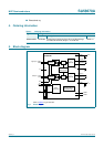
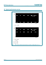
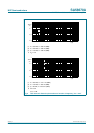
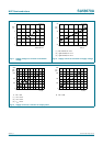
6. Pinning information
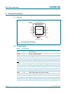
6.1 Pinning
6.2 Pin description
(1) Exposed Die Attach Paddle (DAP).
Fig 2. Pin configuration for HVQFN20
002aad664
SA58670ABS
Transparent top view
OUTRN
PGND
OUTLN
PGND
PVDD PVDD
OUTLP OUTRP
G1 G0
n.c.
SDL
SDR
AVDD
n.c.
INLP
INLN
AGND
INRN
INRP
511
412
313
214
115
6
7
8
9
10
20
19
18
17
16
terminal 1
index area
DAP
(1)
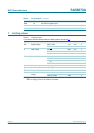
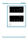
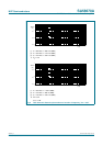
Table 2. Pin description
Symbol Pin Description
G1 1 gain select input 1
OUTLP 2 left channel positive output
PVDD 3 power supply voltage (level same as AVDD)
PGND 4 power ground
OUTLN 5 left channel negative output
n.c. 6 not connected
SDL 7 left channel shutdown input (active LOW)
SDR 8 right channel shutdown input (active LOW)
AVDD 9 analog supply voltage (level same as PVDD)
n.c. 10 not connected
OUTRN 11 right channel negative output
PGND 12 power ground
PVDD 13 power supply voltage (level same as AVDD)
OUTRP 14 right channel positive output
G0 15 gain select input 0
INRP 16 right channel positive input
INRN 17 right channel negative input
AGND 18 analog ground