


26
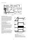
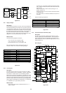
Figure 8-19
8.3.1 Supply Voltages
Description
The CD main board receives +5V and +12V from the CDR main
board via respectively pin 16 and pin 15 of connector 1208. The
+5V is split up into +5VHF and +5V. The +5VHF is used mainly
for the diode currents and the HF-amplifier. The +5V is used for
the digital part of the board. On the board a +3V3 is made from
the +5V for the decoder CD10 and an A3V3 for the DAC
UDA1320. The +12V is split up into A12V for the audio output
stage and +12V for the power drivers of the CDM.
Measurements
Connect following supplies to next pins :
+5V + 5% to pin 16 of connector 1208.
+12V + 5% to pin 15 of connector 1208.
Ground reference to pin 17 of connector 1208.
Keep microprocessor 7202 in reset by forcing pin 7 of
connector 1208 to +5V. Check the following voltages :
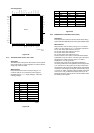
Figure 8-20
8.3.2 Clock Signals
Description
The microprocessor has its own Xtal or resonator of 12MHz.
The CD10 needs a clock of 8.4672MHz + 100ppm. This speed
also relates to the disc speed. To avoid locking problems
between the two drives in the CDR775, both drives run on the
same clock. Therefore the CD main board gets the clock for the
decoder from the CDR main board via pin 2 of connector 1208.
The DAC needs a system clock to drive its internal digital filters
and to clock the I2S signals from the decoder. In our case this
is 11.2896MHz (CL11) generated by the CD10.
Measurements
Connect the power supply as described above in "1.1.1.
Supply Voltages".
Connect on pin 2 of position 1208 a clock signal of 8.4672
MHz ( 100ppm minimum rise time of 50ns and at TTL level
(0V and +5V).
Keep microprocessor 7202 in reset by forcing pin 7 at
position 1208 to +5V.
Release the reset. Now, the processor will reset the CD10
for at least 75
The output clock CL11 should be available now at pin 42 of
the CD10.
Check the following frequencies :
Figure 8-21
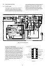
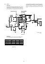
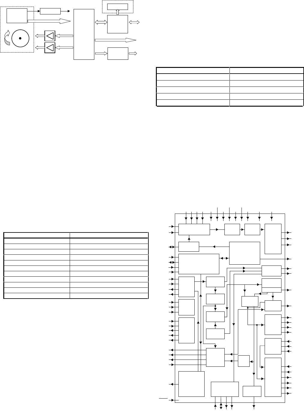
8.3.3 CD10 Decoder/Servo SAA7324 (7000)
Description
The CD10 is a single chip combining the functions of a CD
decoder, digital servo and bitstream DAC. The decoder/servo
part is based on the CD7. The decoding part supports a full
audio specification and can operate at single speed (n=1) and
double speed (n=2).
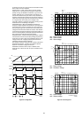
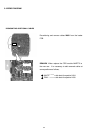
Block Diagram
Figure 8-22
Diode signals
Radial, focus
Motor, sledge
ANA OUT
IIS, DOBM
Trigenta
HF amp.
CD10
SERVO
DECODER
UDA1320
DAC
PROCESSOR
DSA
CDM VAM1250
Loader assy
CL96532086_048.eps
080999
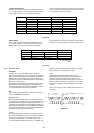
Point Voltage
Position 1000 pins 1,3
+5V
±
5%
Position 7000 pins 5,17,21,57
+3.
3V
±
5%
Position 7005 pin 14
+5V
±
5%
Position 7020 pins 25
+5V
±
5%
Position 7020 pins 26,27,28
+10
±
10%
Position 7021 pin 5
+12V
±
10
Position 7022 pin 5
+12V
±
10
Position 7025 pin 16
+5V
±
5%
Position 7202 pin 38
+5V
±
5% ( other appl. 3V3 possible)
Position 7309 pins 4,13
+3V
3
±
5%
Position 7120 pin 8
+12V
±
10
CL96532086_049.eps
080999
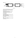
Point Frequency
Position 7000 pin 16
8.4672 MHz
±
100ppm
Position 7202 pins 14,15
12MHz
±
5%
Position 7309 pin 6
11.2896 MHz
±
100ppm
Position 7309 pin 1
2.1168 MHz
±
100ppm
Position 7309 pin2
44.1kHz
±
100ppm
CL96532086_050.eps
080999
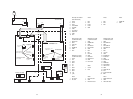
23
19
18
21
20
EFM
DEMODULATOR
MICROCONTROLLER
INTERFACE
CONTROL
PART
V
ref
GENERATOR
V
RIN
ADC
PRE-
PROCESSING
CONTROL
FUNCTION
OUTPUT
STAGES
R1
R2
12
D1 D2 D3 D4
SCL
SDA
FRONT
END
HFIN
HFREF
ISLICE
I
ref
13
7
40
39
2
1
3
6
TEST
TEST1
25
TEST2
31
TEST3
44
TIMING
SELPLL
24
CRIN
16
CROUT
15
CL16
26
CL11/4
49
8910
V
SSA1
V
SSA2
V
DDA1
V
DDA2
V
SSD1
V
SSD3
V
SSD2
V
DDD1(P)
V
DDD2(C)
4 14 5 17 33 50 58 52 57
RA
FO
SL
54
55
56
LDON
64
DIGITAL
PLL
SRAM
RAM
ADDRESSER
SUBCODE
PROCESSOR
SBSY
48
SFSY
47
SUB
46
RCK
45
STATUS
43
DECODER
MICRO-
CONTROLLER
INTERFACE
RESET
38
VERSATILE PINS
INTERFACE
KILL
BITSTREAM
DAC
RP
RN
22
LP
LN
V
pos
V
neg
36
SDI
35
WCLI
37
SCLI
SERIAL
DATA
(LOOPBACK)
INTERFACE
30
EF
27
DATA
28
WCLK
29
SCLK
SERIAL
DATA
INTERFACE
PEAK
DETECT
EBU
INTERFACE
AUDIO
PROCESSOR
ERROR
CORRECTOR
FLAGS
MOTOR
CONTROL
51
DOBM
53
CFLG
MOTO1
59
MOTO2
60
V1
V2/
V3
V4 V5 KILL
63 34 61 62 32
SILD
42
RAB
41
11
CL96532086_051.eps
080999
µs.