20
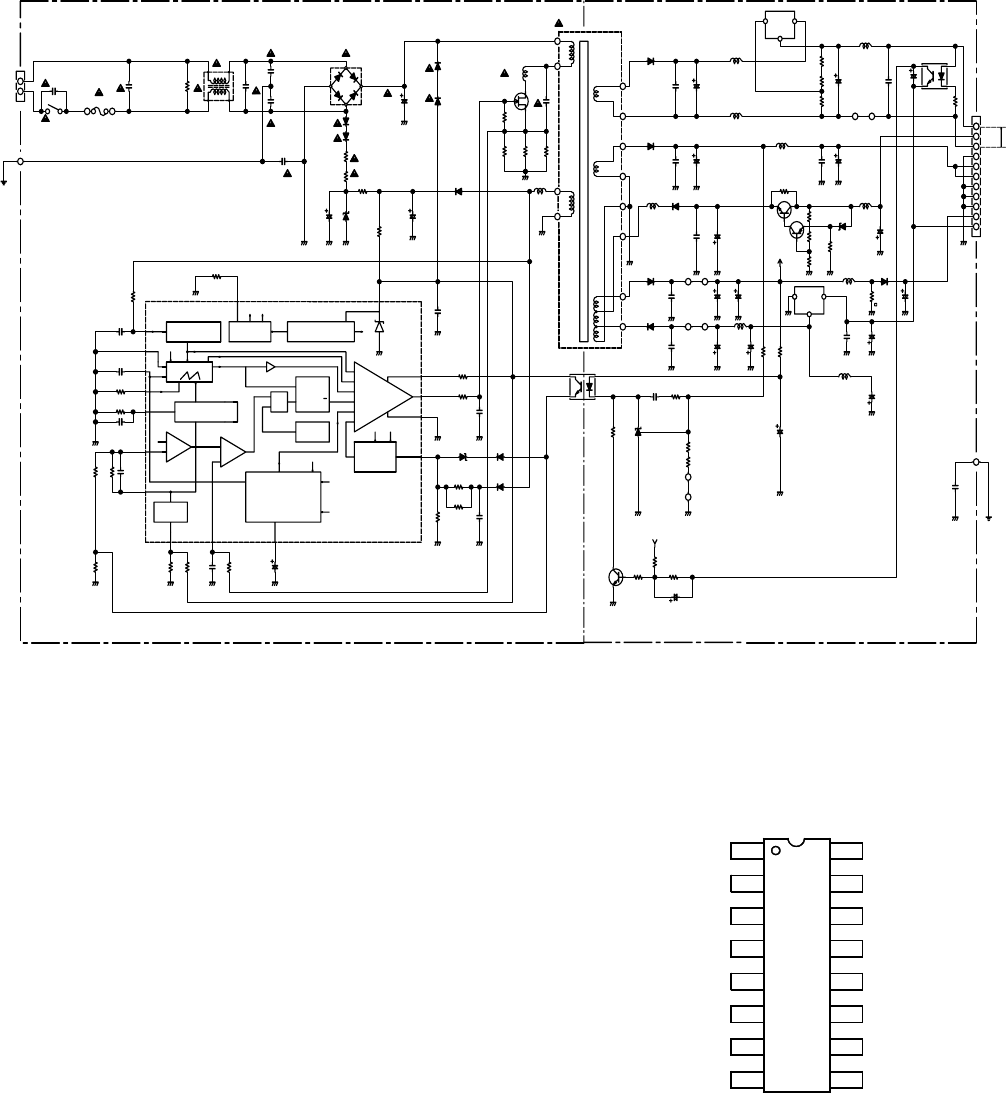
8.2 Power Supply Unit P816
8.2.1 Description of P816
MOSFET Q825 is used as a power switch controlled by the
controller Q810. When the switch is closed, energy is
transferred from mains to the transformer. This energy is
supplied to the load when the switch is opened. Through
control of the switch-on time, the energy transferred in each
cycle is regulated so that the output voltages are independent
of load or input voltage variations. The controlling device
MC44603 is an integrated pulse width modulator. A clock
signal initiates power pulses at a fixed frequency. The
termination of each output pulse occurs when a feedback
signal of the inductor current reaches a threshold set by the
error signal. In this way the error signal actually controls the
peak inductor current on cycle-by-cycle basis.
Figure 8-10 ‘Blockdiagram P816’
Description of controller MC44603
The MC44603 is an enhanced high performance controller that
is specifically designed for off-line and DC-to-DC converter
applications. This device has the unique ability of automatically
changing operating modes if the converter output is
overloaded, unloaded or shorted. The MC44603 has several
distinguishing features when compared to conventional SMPS
controllers. These features consist of a foldback facility for
overload protection, a standby mode when the converter output
is slightly loaded, a demagnetization detection for reduced
switching stresses on transistor and diodes, and a high current
totem pole output ideally suited for driving a power MOSFET. It
can also be used for driving a bipolar transistor in low power
converters. It is optimised to operate in discontinuous mode but
can also operate in continuous mode. Its advanced design
allows use in current mode or voltage mode control
applications.
Pin connections
Figure 8-11
Rref
R Frequency Standby
Voltage feedback Input
Error Amp Output
R Power Standby
Soft-Start/Dmax/
Voltage Mode
Sync Input
Overvoltage Protection (OVP)
Current Sense Input
Demag. Detection
Foldback Input
107
CT
8 9
6
5
11
12
Output
Gnd
VC
VCC
3
4
2
14
13
15
1 16
CL 96532076_030.eps
290799
R832
R823
C825
C828
C826
C859
L852
L854
D836
R886
R884
R885
C866
C871
C861
C851
R819
D835
R803
R826
C827
C898
J891
G815
C821
C881
C875
C869
L853
L851
C860
R851
R852
R853
C855
R810
C873
L872
D829
D832
D814
R808
R801
C801
C802
Q891
C877
L873
L871
L866
D871
D866
D861
D856
D851
D804
D803
R894
C892
Q892
R893
C891
R892
R891
C876
J828
D862
Q871
R887 D881
C882
R883
R882R881
C872
R866
L867
C868
C867
C864
C862
C857
C854
C852
C856
R814
R815
C820
C819
F820
S815
J851
R828
Q851
L831
Q801
D868
L862
R865
R864
R863
R862
Q862
Q861
R861
L861
L856
R802
C803
C804R804R805
R806 R807
C809
R809
C810
C814
R816
C813
R813
R812
C811
L832
R827
R825
L825
Q825
D807
D806
C833
R811
R829
C829
D802
L820
J801
J821
J820
1W
18k
1W
18k
/400V
470pF
/400V
470pF
/400V
470pF
(OPTION)
10µH
1%
2.21k
1%
681
0.1
0.1
0.1
1M(CB)
(UL/CSA,MITI)
330k
4.7k
1
/1kV
470pF
0.1
0.01
/400V
120
/25V
100
/16V
100
/16V
220
4.7µH
4.7µH
0.1
560
220
10
0.1
10k
/16V
220
10µH
24V
AG01
AG01
18k
82k
NP0
82pF
820pF
2SC2878
0.1
10
AG01
RU4YX
AG01
RK46
AG01
1k
100/25
PC123F
10k
100/25
22k
22k
7908
100 TL431
0.022
1.8k
1003.3k/16V
220
1k
2.2µH
/16V
1000
220/50V
10/50V
/10V
2200
100/6.3V
/16V
330
1.8k
1.8k
250V
0.22
250V
0.1
1.5
LM317
PC123F
10µH
10k
10k
10k
1k
2SA
2SC
10k
1µH
6.8µH
22k
470p
4700pF15k15k
1k 180k
1500p
330
2.2/50V
0.1
180
2200pF
15
100
0.1
10
1.5
1k
2SK2943
100/25V
22
10k
4.7/50V
S1WB
2A_125V(F&U )
2A_250V(N&K)
-34V
+4.1V
14
13
12
11
10
9
8
7
6
5
4
1
+12V
+12V
16
8
9
10
15
12
14
13
57
11
6
4
3
2
1
-8V
+12V
GND
GND
GND
+5V
+5V
GND
SWITCHING POWER SUPPLY PCB. (P801)
Q810
L831
UVL01
MC44603P
DETECT
DEMAGINETIZATION
MANAGEMENT
DEMAGNETISATION
OSCILLATOR
STANDBY
(REDUCED FREQUENCY)
IREFVREF
BLOCK
REFERENCE
BLOCKINITIZLIZATION
SUUPLY
IREF
UVL01
Q
LATCH
SHUTDOWN
THERMAL VOCVREF
BUFFER
PROTECT
VOLTAGE
OVER
MANAGEMENT
VOLTAGE
OVER
CURRENT
SENSEINPUT &DMAX
SOFTSTART
CONTROL
SOFT-START
DMAX&
=1
FOLDBACK
INPUT
FOLDBACK
E/A OUT
FEEDBACK
2.5V
OUT
VSB
VREF
VOLTAGE
STANDBY
RP
STANDBY
RF
SYNCIREF
AMP
ERROR


