


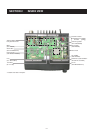
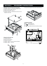
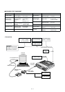

4 - 2
4-1-5 AF AMPLIFIER CIRCUIT (MAIN UNIT)
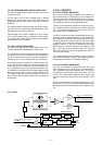
The AF amplifier circuit amplifies the demodulated AF sig-
nals to drive a speaker.
The AF signals from the FM IF IC (IC1, pin 9) are applied to
the active filter circuit (IC16). The active filter circuit (high-
pass filter) removes CTCSS or DTCS signals.
The filtered AF signals are output from pin 14 (IC16) and are
applied to the de-emphasis circuit (R117, C363) with fre-
quency characteristics of –6 dB/octave, and then passed
through the analog switch (IC14, pins 1, 2) and low-pass fil-
ter (IC5 pins 1, 2). The filtered signal is applied to the elec-
tronic volume controller (IC6, pin 9).
The output AF signals from the electronic volume controller
(IC6, pin 10) are passed through the analog switch (IC14
pins 10, 11) and are applied to the AF pre-amplifier (IC15)
and AF power amplifier (IC8) to drive the speaker.
4-1-6 RECEIVER MUTE CIRCUITS (MAIN AND
FRONT UNITS)
• NOISE SQUELCH
The noise squelch circuit cuts out AF signals when no RF
signals are received. By detecting noise components in the
AF signals, the squelch circuit switches the AF mute switch.
Some noise components in the AF signals from the FM IF IC
(IC1, pin 9) are passed through the level controller (IC6, pins
1, 2). The level controlled signals are applied to the active fil-
ter section in the FM IF IC (IC1, pin 8) as “SQLIN” signal.
Noise components about 10 kHz are amplified and output
from pin 7.
The filtered signals are converted to the pulse-type signals
at the noise detector section and output from pin 13 (NOIS).
The “NOIS” signal from the FM IF IC is applied to the CPU
(FRONT unit; IC1, pin 53). The CPU then analyzes the noise
condition and controls the AF mute signal via “AFON” line
(FRONT unit; IC1, pin 43) to the AF regulator (Q35, Q36,
D29, D30).
• CTCSS AND DTCS
The tone squelch circuit detects AF signals and opens the
squelch only when receiving a signal containing a matching
subaudible tone (CTCSS or DTCS). When tone squelch is in
use, and a signal with a mismatched or no subaudible tone
is received, the tone squelch circuit mutes the AF signals
even when noise squelch is open.
A portion of the AF signals from the FM IF IC (IC1, pin 9)
passes through the low-pass filter (IC16) to remove AF
(voice) signals and is applied to the CTCSS or DTCS
decoder inside the CPU (FRONT unit; IC1, pin 50) via the
“CDEC” line to control the AF mute switch.
4-2 TRANSMITTER CIRCUITS
4-2-1 MICROPHONE AMPLIFIER CIRCUIT
(MAIN AND FRONT UNITS)
The microphone amplifier circuit amplifies audio signals
within +6 dB/octave pre-emphasis characteristics from the
microphone to a level needed for the modulation circuit.
The AF signals (MIC) from the MIC jack (FRONT unit; J1)
are amplified at the AF amplifier (FRONT unit; IC5) and
applied to the MAIN unit via J2 (pin 13). The AF signal are
applied to the limiter amplifier (IC5, pin 5).
The entered signals are pre-emphasized with +6dB/octave
at a limiter amplifier, then passed through the analog switch
(IC14, pins 4, 3) and splatter filter (IC5, pins 2, 1). The out-
put signals from the splatter filter are applied to the level
controller (IC6, pins 9, 10).
The deviation level controlled signals are then applied to the
modulation circuit (D18) as the “MOD” signal after being
passed through the analog switch (IC14, pins 9, 8).
4-2-2 MODULATION CIRCUIT (MAIN UNIT)
The modulation circuit modulates the VCO oscillating signal
(RF signal) using the microphone audio signals.
The AF signals from the analog switch (IC14, pin 8) change
the reactance of varactor diode (D18) to modulate the oscil-
lated signal at the TX VCO circuit (Q13, D16, D31). The
modulated VCO signal is amplified at the buffer amplifiers
(Q11, Q10) and is then applied to the drive amplifier circuit
via the T/R switch (D14).
The CTCSS/DTCS signals from the CPU (FRONT unit; IC1,
pins 13, 14, 19, 20) are passed through the low-pass filter
(FRONT unit; IC5), and mixer and splatter filter (IC5), and
are then applied to the VCO circuit.
4-2-3 DRIVE AMPLIFIER CIRCUIT (MAIN UNIT)
The drive amplifier circuit amplifies the VCO oscillating sig-
nal to the level needed at the power amplifier.
The RF signal from the buffer amplifier (Q10) passes
through the T/R switch (D14) and is amplified at the drive
amplifier circuit (Q8). The amplified signal is applied to the
power amplifier circuit.