


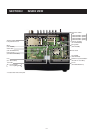
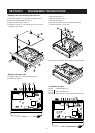
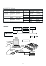
4 - 3
4-2-4 POWER AMPLIFIER CIRCUIT (MAIN UNIT)
The power amplifier circuit amplifies the driver signal to an
output power level.
The RF signal from the drive amplifier (Q8) is passed
through the low-pass filter circuit (L18, C90, C89) and
applied to the power module (IC3) to obtain 25 W or 45 W of
RF power.
The amplified signal is passed through the antenna switch-
ing circuit (D2, D3), low-pass filter and APC detector, and is
then applied to the antenna connector.
Control voltage for the power amplifier (IC3, pin 2) comes
from the APC amplifier (IC2) to stabilize the output power.
The transmit mute switch (D28) controls the APC amplifier
when transmit mute is necessary.
4-2-5 APC CIRCUIT (MAIN UNIT)
The APC circuit protects the power amplifier from a mis-
matched output load and stabilizes the output power.
The APC detector circuit detects forward signals and reflec-
tion signals at D1 and D11 respectively. The combined volt-
age is at minimum level when the antenna impedance is
matched at 50 Ω, and is increased when it is mismatched.
The detected voltage is applied to the APC amplifier (IC2,
pin 3), and the power setting “T2” signal from the D/A con-
verter (IC6, pin 22), controlled by the CPU (FRONT unit;
IC1), is applied to the other input for reference. When anten-
na impedance is mismatched, the detected voltage exceeds
the power setting voltage. Then the output voltage of the
APC amplifier (IC2, pin 4) controls the input current of the
drive amplifier (Q8) and power module (IC3) to reduce the
output power.
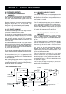
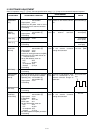
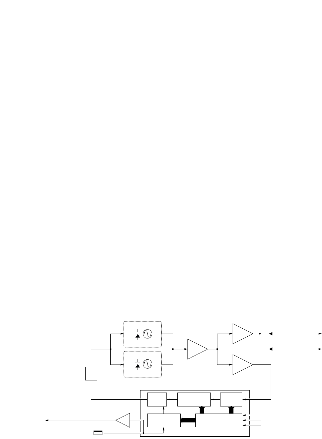
4-3 PLL CIRCUITS
4-3-1 PLL CIRCUIT (MAIN UNIT)
A PLL circuit provides stable oscillation of the transmit fre-
quency and receive 1st LO frequency. The PLL output com-
pares the phase of the divided VCO frequency to the refer-
ence frequency. The PLL output frequency is controlled by
the divided ratio (N-data) of a programable divider.
The PLL circuit contains the TX/RX VCO circuit (Q14, Q13).
The oscillated signal is amplified at the buffer amplifiers
(Q11, Q12) and then applied to the PLL IC (IC4, pin 8) via
the low-pass filter (L32, C299, C300).
The PLL IC contains a prescaler, programable counter, pro-
gramable divider and phase detector, etc. The entered sig-
nal is divided at the prescaler and programable counter sec-
tion by the N-data ratio from the CPU. The reference signal
is generated at the reference oscillator (X2) and is also
applied to the PLL IC. The PLL IC detects the out-of-step
phase using the reference frequency, and outputs it from
pin 5. The output signal is passed through the loop filter
(R96/C130/C147, R95/C146), and is then applied to the
VCO circuit as the lock voltage.
If the oscillated signal drifts, its phase changes from that of
the reference frequency, causing a lock voltage change to
compensate for the drift in the oscillated frequency.
4-3-2 VCO CIRCUIT (MAIN UNIT)
The VCO circuit contains a separate RX VCO (Q13, D16)
and TX VCO (Q14, D17). The oscillated signal is amplified
at the buffer amplifiers (Q11, Q10) and is then applied to the
T/R switch circuit (D14, D15). Then the receive 1st LO (RX)
signal is applied to the 1st mixer (Q3) and the transmit (TX)
signal to the drive amplifier circuit (Q8).
A portion of the signal from the buffer amplifier (Q11) is fed
back to the PLL IC (IC4, pin 8) via the buffer amplifier (Q12)
and low-pass filter (L32, C299, C300) as the comparison
signal.
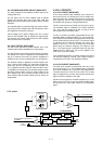
• PLL circuit
Shift register
×3
Prescaler
Phase
detector
Loop
filter
Programmable
counter
Programmable
divider
X2
15.3 MHz
2nd LO signal to the FM IF IC
45.9 MHz
1
2
Buffer
Q11
Buffer
Q10
Buffer
Q12
Tripler
9
10
11
SCK
SO
PLST
to transmitter circuit
to 1st mixer circuit
D14
D15
5
8
Q34
IC4 MB15A02PFV1
Q14, D17
TX VCO
Q13, D16
RX VCO