


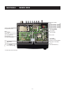
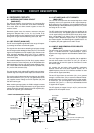
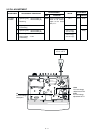
4-4 POWER SUPPLY CIRCUITS
4-4-1 VOLTAGE LINES (MAIN UNIT)
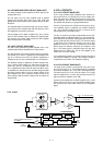
4-5 PORT ALLOCATIONS
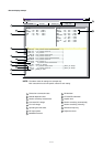
4-5-1 LED DRIVER (FRONT UNIT; IC4)
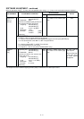
4-5-2 OUTPUT EXPANDER (MAIN unit; IC6)
4-5-3 CPU (FRONT UNIT; IC1)
Output LEDs control signals.
Low : While LEDs are ON.
Outputs BUSY LED control signal.
Outputs TX LED control signal.
Outputs LED bright control signal.
Outputs backlight control signal.
Outputs external device control signal.
High :
When matched 5/2 tone signals
are received.
4 - 4
Description
The voltage from a DC power supply.
The same voltage as the HV line which is con-
trolled by the power switching circuit (Q23, Q24).
When the [POWER] switch is pushed, the CPU
outputs the “PWON” control signal to the power
switching circuit to turn the circuit ON.
Common 5 V for the CPU converted from the HV
line by the CPU5V regulator circuit (IC10). The
circuit outputs the voltage regardless of the
power ON/OFF condition.
Common 8 V converted from the VCC line by the
8V regulator circuit (IC9).
Common 5 V converted from the VCC line by the
5V regulator circuit (Q27, Q28).
Receive 8 V controlled by the R8 regulator circuit
(Q26, Q30) using the “RXC” signal from the CPU
(FRONT unit; IC1, pin 18).
Transmit 8 V controlled by the T8 regulator circuit
(Q25, Q29, D23) using the “TMUT” signal from
the CPU (FRONT unit; IC1, pin 40).
Line
HV
VCC
CPU5V
8V
5V
R8V
T8V
Input port for the internal temperature.
Input port for low voltage detection
from the connected power supply.
Input port for the reset signal.
Output ports for 5/2 tone and DTMF
signals.
Outputs the CPU clock shift signal.
Outputs the cut-off frequency control
signal to the low-pass filter (MAIN; unit
IC5) for CTCSS/DTCS switching.
Input port for the PLL unlock signal
from the PLL IC (MAIN unit; IC4).
Outputs the R8V regulator circuit
(MAIN unit; Q26, Q30) control signal.
Output ports for 5/2 tone and DTMF
signals.
Input ports for key matrix.
Output ports for CTCSS/DTCS signals.
Input ports for key matrix.
Outputs clock signal to the PLL IC
(MAIN unit; IC4), D/A converter (MAIN
unit IC6), LED driver (FRONT unit; IC4)
and optional board (connect to MAIN
unit; J1).
Outputs data signal to the PLL IC
(MAIN unit; IC4), D/A converter (MAIN
unit; IC6), LED driver (FRONT unit;
IC4) and optional board (connect to
MAIN unit; J1).
Output port for beep sound signal.
I/O port for the data signal for the EEP-
ROM (FRONT unit; IC3)
Outputs clock signal for the EEPROM
(FRONT unit; IC3).
Input port for the MIC mute signal from
the optional board via MAIN unit, J1.
Input port for the AF mute signal from
the optional board via MAIN unit, J1.
Outputs strobe signal for the PLL IC
(MAIN unit; IC4).
Outputs strobe signal for the D/A con-
verter IC (MAIN unit; IC6).
Outputs strobe signal for LED driver IC
(FRONT unit; IC4).
Outputs control signal for the LED dri-
ver IC (FRONT unit; IC4).
Outputs the T8V regulator circuit
(MAIN unit; Q25, Q29, D23) control
signal.
1
2
7
13, 14
15
16
17
18
19, 20
21, 22
23–25
26, 27
28
29
30
31
32
33
34
36
37
38
39
40
TEMP
BATV
RES
SENC0,
SENC1
CSFT
DUSE
UNLK
RXC
SENC0,
SENC1
P0, P1
CENO0–
CENO2
P2, P3
SCK
SO
BEEP
ESDA
ESCL
MMUT
RMUT
PLST
DAST
EXST
EXOE
TMUT
Pin Port
Description
number name
Outputs squelch control signal.
Outputs deviation (Tone) control signal.
Outputs deviation control signal.
Outputs DTCS control signal.
Outputs RX BPF control signal.
Outputs AGC control signal.
Outputs TX RF power control signal.
Outputs PLL reference control signal.
2
3
10
11
14
15
22
23
VOUT1
VOUT2
VOUT3
VOUT4
VOUT5
VOUT6
VOUT7
VOUT8
Pin Port
Description
number name
5–11
14
15
16
17
18
CH1–CH4
LP0–LP2
RLED
TLED
LIGT1
LIGT2
HORN
Pin Port
Description
number name