


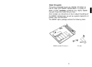


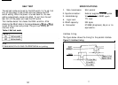


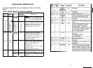
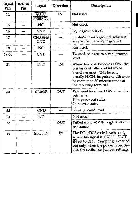
HARDWARE DESCRIPTION
For signal description and pin assignment, refer to the table
below:
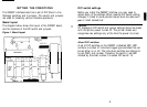
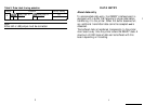
Table 5. Signal description and pin assignment
I
Signal
Pin
I
izn
Pin
19
-
Signal
YimiE
I
Ike&on
Description
IN
STROBE pulse to read data. Pulse
width must be more than 0.5 micro-
seconds at the receiving
terminal.
12
13
20
21
22
23
24
25
26
27
30
-
DATA 1
IN
These signals represent information
DATA 2
IN
of the 1st to 8th bits of parallel data,
DATA 3 IN
respectively. Each signal is at
DATA 4
IN
HIGH level when data is logical 1
DATA 5
IN
and LOW when it is logical 0.
DATA 6 IN
DATA 7
IN
DATA 8
IN
vXNLG
OUT
About a IO-microsecond pulse.
LOW indicates that data has been
received and that the interface
board is ready to accept more data.
This signal is output as a pair
together with BUSY.
BUSY
OUT
A HIGH signal indicates that the
interface board cannot receive data.
The signal goes HIGH in the
following cases:
SLCT
L
1) During data entry (ea. car. time)
2) When off line
OUT
OUT
3) During printer-error state
A HIGH signal indicates that the
printer is out of paper.
Pulled up to +5 V through 3.3k ohm
resistance.
12
13