


Getting Started With SHARC Processors 1-5
Introduction to SHARC Processors
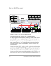
• An SDRAM controller that provides an interface to as many as four
separate banks of industry-standard SDRAM devices
• Up to a maximum of 5M bits of on-chip SRAM and up to 4M bits
of on-chip, mask-programmable ROM
• Input/output processor (IOP) with integrated direct memory
access (DMA) controller, serial peripheral interface (SPI) compati-
ble port, and serial ports (SPORTs) for point-to-point
multiprocessor communications
• A variety of audio-centric peripheral modules including a
Sony/Philips digital interface (S/PDIF), sample rate converter
(SRC), and pulse width modulation (PWM)
• JTAG test access port for emulation
Figure 1-1 also shows the three on-chip buses of the
ADSP-21472/21475/21479 processors: the PM bus, DM bus, and I/O
bus. The PM bus provides access to instructions or data. During a single
cycle, these buses let the processor access two data operands from memory,
access an instruction (from cache), and perform a DMA transfer. In addi-
tion, Figure 1-1 shows the asychronous memory interface available on the
ADSP-2147x processors.
Four Generations of SHARC Processors
The SHARC architecture has a long history in the floating-point proces-
sor market. While architectural enhancements have been made with each
successive processor generation, the common traits of exceptional float-
ing-point performance, matched to high-bandwidth memory and I/O
transfers, remains. All four generations of SHARC processors are still in
production, offering a variety of code-compatible options to meet a wide
array of price, performance, and footprint requirements.