


– 31 – – 32 –
MZ-R70
1
A
B
C
D
E
F
G
H
I
234567891011
TP904
C638
R619
C632
C525
C925
L901
LF901
TH901
D907
C930
C905
C917
C915
L903
C528
C527
C617
C618
C616
FB505
C304
L301
C303
C202
C113
C103
C102
C334
C625
C623
C624
R525
R636
C640
R526
S802
(OPEN)
R815
R811
R834
R835
R808
R806
R840
R805
R803
R802
R801
R614
C600
R814
R812
R938
R928
C921
R927
R931
R934
R912
R919
R908
R903
R203
R208
R223
C926
R528
C510
R524
R321
TP344
TP315
TP343
TP333
TP332
RB603 RB602
C220
C222
C203
D101 D201
TP331 TP334
TP341
TP335
TP342
L501
CN501
L902
TP5112
AP5101
AP5102
TP5120
R204
R104
R102
TP347
TP348
D905
TP903
C122
R301
R202
C307
C333
C106
C308
R201
C120
R325
C913
C524
R101
R322
R930
L905
L904
L603
Q905
C933
C932
C935
C922
TP823
C923
C934
D906
R907
C206
C902
111-677-124-
TP905
TP906
TP311
TP312
TP313
TP314
TP316
TP317
TP336
TP337
TP346
TP345
TP338
C201
R209
R921
R307
R302
C534
R520
C536
R522
R838
TP828
AP808
TP5118
AP5119
TP914
TP915
R942
R929
R937
R936
C918
C910
C929
R923
R924
R913
R612
R639
TP601
04
D600
D601
Q603
R611
C612
R637
L606
C605
C613
C615
C614
C601
C602
R613
D602
R809
R813
R807
TP816
AP909
AP910
C810
S803
T.MARK
OPTICAL
PICK-UP
TP9001
TP801
C535
FB601
IC504 IC505
C629
85
14
85
14
C514
IC601
AP530
TP5105
L601
C621
L604
X501
C631
R638
S801
(OPEN/CLOSE)
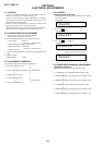
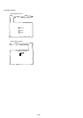
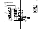
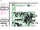
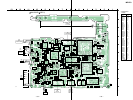
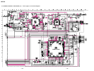
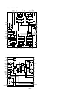
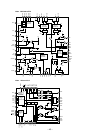
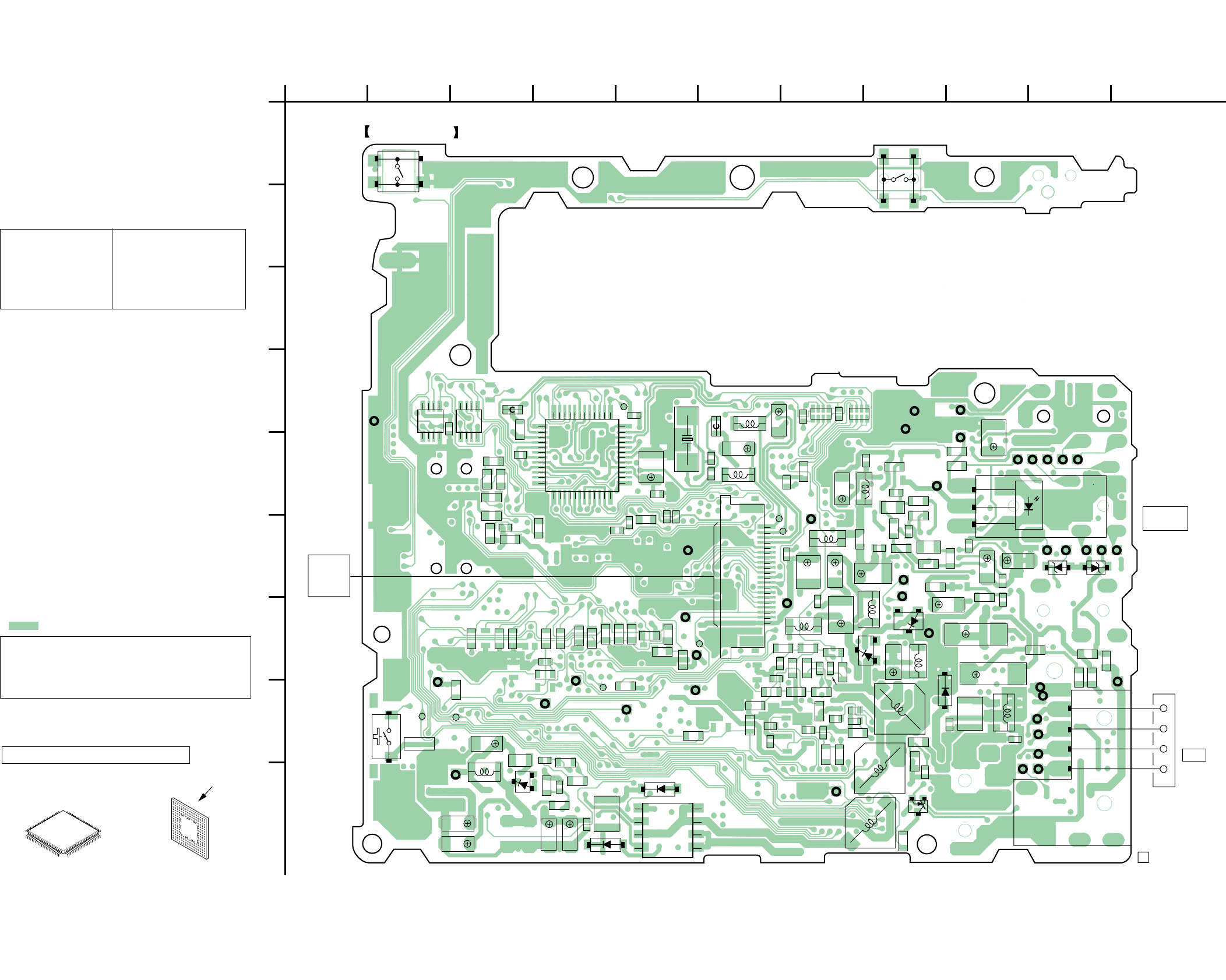
MAIN BOARD (SIDE A)
1
4
8
5
1
5
10
1520
25
30
35
40 45 48
1
10
20
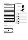
J304
(1/2)
J301
(1/2)
LINE IN
(OPTICAL)
i 1
(LINE OUT)
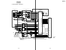
Common note on Printed Wiring Boards:
• Y : parts extracted from the conductor side.
•
f
: internal component.
• : Pattern from the side which enables seeing.
Caution:
Pattern face side: Parts on the pattern face side seen from the
(Side B) pattern face are indicated.
Parts face side: Parts on the parts face side seen from the
(Side A) parts face are indicated.
• Main board is four-layer printed board.
However, the patterns of layers 2 and 3 have not been in-
cluded in this diagrams.
*
IC502, IC801 is not replaceable
• Lead Layouts
surface
Lead layout of conventional IC CSP (chip size package)
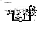
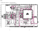
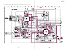
Common note on Schematic Diagram:
• All capacitors are in µF unless otherwise noted. pF: µµF
50 WV or less are not indicated except for electrolytics
and tantalums.
• All resistors are in Ω and
1
/4
W or less unless otherwise
specified.
• % : indicates tolerance.
•
f
: internal component.
• C : panel designation.
• A : B+ Line.
• Power voltage is dc 3V and fed with regulated dc power
supply from external power voltage jack.
• Voltages and waveforms are dc with respect to ground in
playback mode.
no mark : REC
( ) : PB
∗
: Impossible to measure
• Voltages are taken with a VOM (Input impedance 10 MΩ).
Voltage variations may be noted due to normal produc-
tion tolerances.
• Waveforms are taken with a oscilloscope.
Voltage variations may be noted due to normal produc-
tion tolerances.
• Circled numbers refer to waveforms.
• Signal path.
J : CD
Note:
The components identi-
fied by mark 0 or dotted
line with mark 0 are criti-
cal for safety.
Replace only with part
number specified.
Note:
Les composants identifiés par
une marque 0 sont critiques
pour la sécurité.
Ne les remplacer que par une
piéce portant le numéro
spécifié.
6-4. PRINTED WIRING BOARD — MAIN BOARD —