


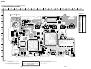
– 14 –
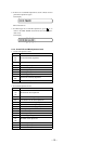
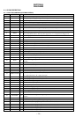
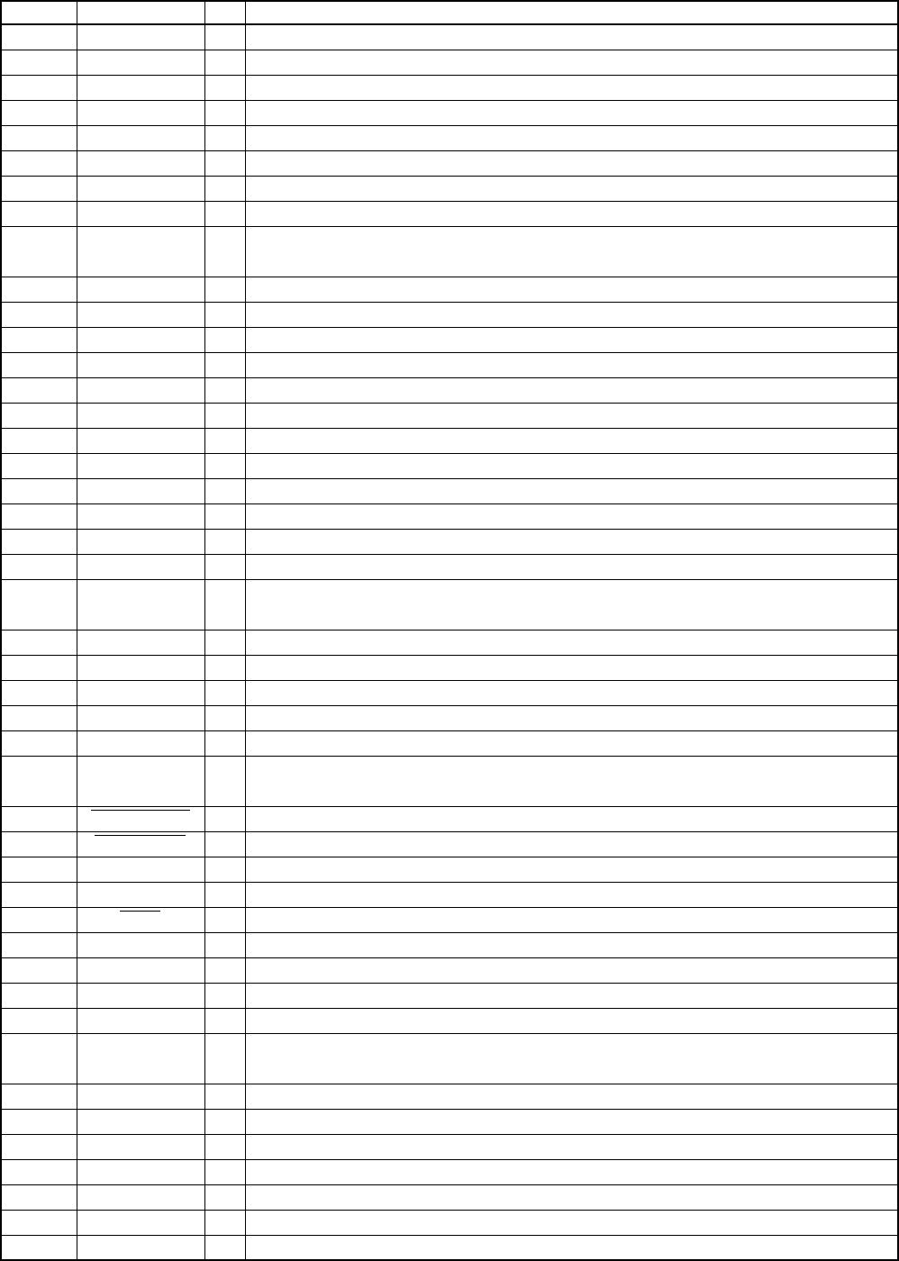
Pin No. Pin Name I/O Description
1 S MON I S-MON monitor signal input from the µPD63732GC (IC601)
2 UREG MON I Un-regulator power supply voltage monitor input terminal (A/D input)
3NC— Not used. (open)
4 VREF I Input terminal for power supply voltage adjustment reference voltage (+2 V) (A/D input)
5 DVDD MON I Not used. (Fixed at “H”.)
6NC— Not used. (open)
7 RMC KEY I Remote commander with headphone key input terminal (A/D input)
8 SET KEY I Set key input terminal (A/D input) S801 to S804 (x, >/N, ., +/– VOLUME keys input)
9 MRST I
System reset signal input “L”: reset
For several hundreds msec. after the power supply rises, “L” is input, then it change to “H”
10 AVDD — Power supply pin (+2.4 V or +2.8 V)
11 AVSS — Ground terminal (for A/D converter)
12 – 15 TYPE0 – 3 I Setting terminal for model discrimination (bit 0 to bit 3) Fixed at “L” in this set
16 XOUT O Main system clock output terminal (16.9344 MHz)
17 XIN I Main system clock input terminal (16.9344 MHz)
18 SX OUT O Sub system clock output terminal Not used. (open)
19 SXIN I Sub system clock input terminal Not used. (fixed at “L”)
20 COUT O Not used. (open)
21 VDD — Power supply terminal (+2 V) (digital system)
22 VSS — Ground terminal (digital system)
23 HOLD SW I HOLD switch (S808) input terminal “L”: hold off, “H”: hold on
24 VG CON O Power supply control signal output to each ICs
25 XCLK O
System clock supply output terminal (16.934 MHz) to the µPD63732GC (IC601) or AK4352
(IC302)
26 KEY EN O Ground control output terminal of remote control
27 AVLS SW I AVLS switch (S803) input terminal “L”: LIMIT “H”: NORM
28 DSP SINT I Interruption status input from the µPD63732GC (IC601)
29, 30 DBB0, DBB1 I DIGITAL MEGABASS switch (S806) input terminal *1
31 OPR LED O OPERATE LED (D802) drive signal output terminal “H”: LED on
32 OPEN CLS SW I
Upper panel open/close detect switch (S801) input terminal
“L”: upper panel close, “H” : upper panel open
33 XWAKE RMC I Wake up signal input from remote control key
34 XWAKE SET I Wake up signal input from this set key
35 SBUS CLK O SSB serial clock signal output terminal
36 SBUS DATA I/O SSB serial data input/output terminal
37 XRST O Reset signal output terminal to each ICs
38 SLD 1 MON I Sled servo timing signal input from the TLC372CPW (IC552)
39 SLD 2 MON I Sled servo timing signal input from the TLC372CPW (IC552)
40 VDD — Power supply terminal
41 VPP — Test terminal (fixed at “L”)
42 CLV VCON O
Spindle servo drive voltage control signal output to the BD6602KUT (IC551) or µPD63732GC
(IC601)
43 APC REF O Laser power control signal output terminal
44 RM VCON O Remote control power voltage select signal output to power circuit “L”:2.4 V, “H”: 2.8 V
45 CLV U MON I Spindle servo (U) timing signal input from the BD6602KUT (IC551)
46 CLV V MON I Spindle servo (V) timing signal input from the BD6602KUT (IC551)
47 CLV W MON I Spindle servo (W) timing signal input from the BD6602KUT (IC551)
48 CLV U CON I Spindle servo (U) drive signal input from the BD6602KUT (IC551)
49 CLV V CON I Spindle servo (V) drive signal input from the BD6602KUT (IC551)
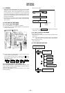
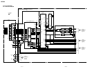
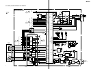
SECTION 6
DIAGRAMS
6-1. IC PIN DESCRIPTION
6-1-1. IC801 RU6915MF-0006 (SYSTEM CONTROL)