


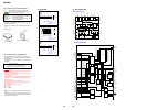
2222
MZ-E900
r
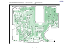
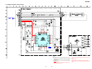
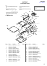
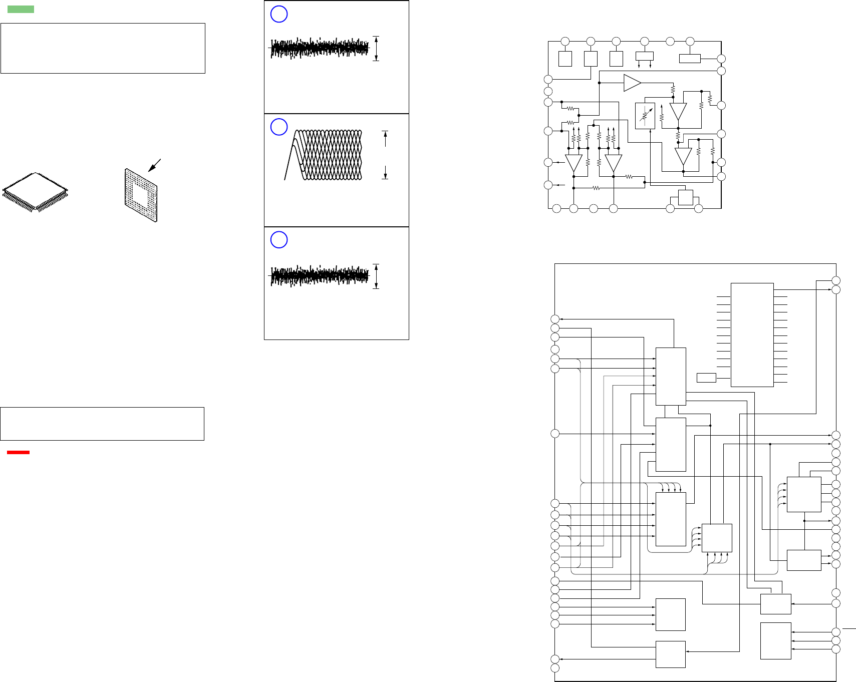
WAVEFORMS
1
IC501 1 TE
2
3
IC501 ed (RF)
IC501 rs (FE)
Approx.
12 mVp-p
Approx.
1.2 Vp-
p
Approx.
10 mVp-p
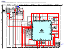
Note on Schematic Diagram: MAIN SECTION
• All capacitors are in µF unless otherwise noted. pF: µµF
50 WV or less are not indicated except for electrolytics
and tantalums.
• All resistors are in Ω and
1
/
4
W or less unless otherwise
specified.
•
f
: internal component.
Note: The components identified by mark 0 or dotted
line with mark 0 are critical for safety.
Replace only with part number specified.
• : B+ Line.
• Power voltage is dc 1.5V and fed with regulated dc power
supply from battery terminal.
• Voltages and waveforms are dc with respect to ground
under no-signal conditions.
no mark : PLAY
• Voltages are taken with a VOM (Input impedance 10 MΩ).
Voltage variations may be noted due to normal produc-
tion tolerances.
• Waveforms are taken with a oscilloscope.
Voltage variations may be noted due to normal produc-
tion tolerances.
• Circled numbers refer to waveforms.
• Signal path.
F : Analog
J : Digital
• Replacement of IC601 used in this set requires a special
tool.
• The voltage and waveform of CSP (chip size package)
cannot be measured, because its lead layout is different
form that of conventional IC.
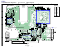
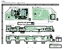
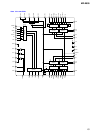
Note on Printed Wiring Boards: MAIN SECTION
• X : parts extracted from the component side.
• : Pattern from the side which enables seeing.
(The other layers' patterns are not indicated.)
Caution:
Pattern face side: Parts on the pattern face side seen from the
(Side B) pattern face are indicated.
Parts face side: Parts on the parts face side seen from the
(Side A) parts face are indicated.
• Main boards is four-layer printed board.
However, the patterns of layer 2 and 3 have not been
included in this diagrams.
• Replacement of IC601 used in this set requires a special
tool.
• Lead Layouts
Lead layout of
conventional IC
surface
CSP (chip size package)
r
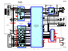
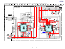
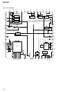
IC BLOCK DIAGRAMS
IC301 TA2131FL-EL
V REF
MT
SW
BST
SW
BEEP
19
20
21
22
23
24
18 17 16 15 14 13
PW
SW
12
11
10
8
7
BST1
9
BST2
654321
BST
AGC
PW
B
PW
A
ADD
TC MT
VCC
INR
INL
BEEP
OUTB
BEEP
OUTA
+B
OUTL
PWR
GND
OUTR
DET
AGC IN
BST OUT
BST NF2
LPF2
BST NF1
LPF1
VREF
VREF IN
GND
BEEP IN
BST SW
MUTE
STB
IC501 SN761057DBT
1
TE
REXT
Wpp-LPF
VREF
C
D
D-C
Iy
Ix
Jx
Jy
A
A-C
B
ADIP-IN
FE
ABCD
AVCC
OFC-1
OFC-2
PS
LP
EQ
AGND
RF
CCSL2
VC
XRST
SCK
SBUS
VREF075
PEAK
BOTM
DGND
OFTRK
S-MON
TON-C
CIG
CDN
ADFG
DVDD
PD-NI
PD-I
PD-O
43
44
TWpp
PK/BTM
Aw
CSLO
VREF075
A-C
D-C
Malfa
Mij
AwBPF
Dw
DwBPF
42
38
37
36
35
34
31
30
29
28
27
26
25
24
23
39
41
40
2
3
4
5
6
7
8
9
10
11
12
13
14
15
16
17
18
19
20
21
22
A+B+C+D
I+J
NPP
TON
CSL
Aw+Dw
TON Peak
TON Botm
ADIP
TE
TEMP
33
32
S-MONITOR
TE
RF
FE
APC
ADIP
T-ON
SERIAL
I/F
PEAK/BOTM
ABCD
Tpp/Wpp
VOLT/DIV : 5 mV AC
TIME/DIV : 1 µsec
VOLT/DIV : 0.5 V AC
TIME/DIV : 0.5 µsec
VOLT/DIV : 5 mV AC
TIME/DIV : 1 µsec