


2121
HCD-XGR6/XGR60
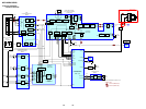
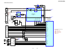
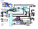
Note on Schematic Diagram:
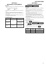
• All capacitors are in µF unless otherwise noted. pF: µµF
50 WV or less are not indicated except for electrolytics
and tantalums.
• All resistors are in Ω and
1
/
4
W or less unless otherwise
specified.
•
2
: nonflammable resistor.
• 5 : fusible resistor.
• C : panel designation.
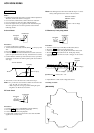
Note on Printed Wiring Boards:
• X : parts extracted from the component side.
• : Pattern from the side which enables seeing.
(The other layers´ Patterns are not indicated.)
• Indication of transistor.
• A : B+ Line.
• B : B– Line.
• H : adjustment for repair.
• Voltages and waveforms are dc with respect to ground
under no-signal conditions.
BD board section
no mark: CD PLAY
Other board section
no mark: TUNER (FM/AM)
( ): TAPE PLAY
< >: TAPE REC
[ ]: CD PLAY
• Voltages are taken with a VOM (Input impedance 10 MΩ).
Voltage variations may be noted due to normal produc-
tion tolerances.
• Waveforms are taken with a oscilloscope.
Voltage variations may be noted due to normal produc-
tion tolerances.
• Circled numbers refer to waveforms.
• Signal path.
F : TUNER (FM/AM)
E : TAPE PALY (DECK A)
d : TAPE PALY (DECK B)
G : RECORD
J : CD PALY (ANALOG OUT)
c : CD PALY (DIGITAL OUT)
N : MIC INPUT
• Abbreviation
AR : Argentina model
MX : Mexican model
E51 : Chilean and Peruvian model
Note:
The components identified by mark 0 or dotted line
with mark 0 are critical for safety.
Replace only with part number specified.
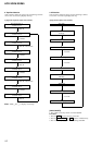
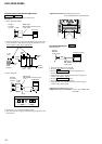
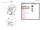
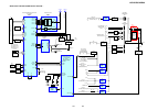
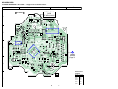
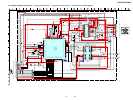
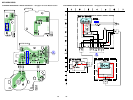
SECTION 6
DIAGRAMS
PANEL FL board
TRANS board
SUB TRANS board
MAIN boar
d
PA board
TC-B board
HEADPHONE board
FRONT INPUT board
CD-R board
SENSOR board
D-SW board
MOTOR board
LED board
BD board
CD-L board
MIC/GUITAR board
TC-A board
PANEL VR board
TUNER PACK
(FM/AM TUNER UNIT)
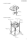
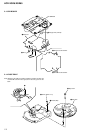
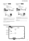
6-1. CIRCUIT BOARD LOCATION
B
These are omitted.
CE
Q
B
These are omitted.
CE
Q
C
B
These are omitted.
E
Q