


15 15
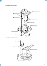
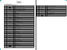
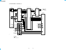
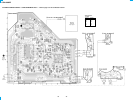
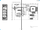
DISC IN SW board
DISPLAY board
LOAD SW board
SERVO board
MAIN board
LIMIT SW board
SUB board
4-5. CIRCUIT BOARDS LOCATION
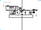
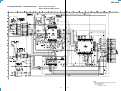
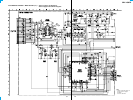
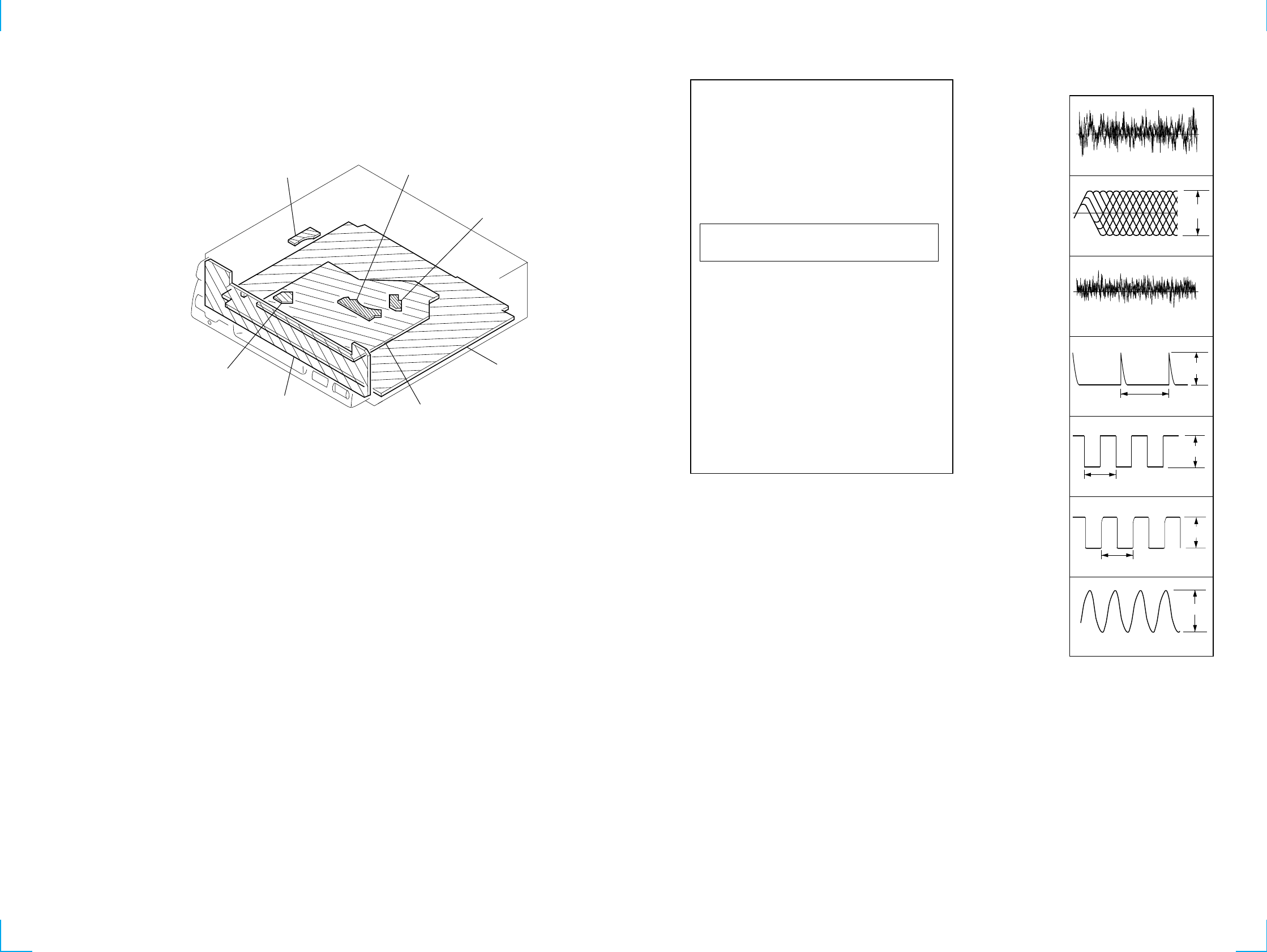
• Waveforms (MODE:PLAY)
1
2
3
4
5
6
7
Approx. 620mVp-p
IC2
1
(FEO)
0V
IC2
ea
(RFO)
1.2Vp-p
Approx. 200mVp-p
IC2
rs
(TEO)
0V
IC1
3
(MDP)
2.6Vp-p
7.6µsec
IC1
w;
(LRCK)
5.8Vp-p
22.7µsec
IC1
ws
(BCK)
5.7Vp-p
474nsec
16.89MHz
IC1
ef
(XTAI)
3.2Vp-p
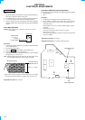
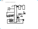
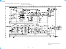
THIS NOTE IS COMMON FOR PRINTED WIRING
BOARDS AND SCHEMATIC DIAGRAMS.
(In addition to this, the necessary note is
printed in each block.)
for schematic diagram:
• All capacitors are in µF unless otherwise noted. pF: µµF
50 WV or less are not indicated except for electrolytics
and tantalums.
• All resistors are in Ω and
1
/
4
W or less unless otherwise
specified.
• % : indicates tolerance.
• C : panel designation.
• U : B+ Line.
• H : adjustment for repair.
• Power voltage is dc 14.4V and fed with regulated dc power
supply from ACC and BATT cords.
• Voltages are taken with a VOM (Input impedance 10 MΩ).
Voltage variations may be noted due to normal produc-
tion tolerances.
• Waveforms are taken with a oscilloscope.
Voltage variations may be noted due to normal produc-
tion tolerances.
• Circled numbers refer to waveforms.
• Signal path.
F : FM
f : AM
J : CD
for printed wiring boards:
• X : parts extracted from the component side.
• b : Pattern from the side which enables seeing.
Note: The components identified by mark 0 or dotted line
with mark 0 are critical for safety.
Replace only with part number specified.